
1
Æ
FN7177.1
EL5144, EL5146, EL5244, EL5246, EL5444
100MHz Single-Supply Rail-to-Rail
Amplifiers
The EL5144 series amplifiers are voltage-feedback, high
speed, rail-to-rail amplifiers designed to operate on a single
+5V supply. They offer unity gain stability with an unloaded -
3dB bandwidth of 100MHz. The input common-mode voltage
range extends from the negative rail to within 1.5V of the
positive rail. Driving a 75
double terminated coaxial cable,
the EL5144 series amplifiers drive to within 150mV of either
rail. The 200V/µs slew rate and 0.1%/0.1
∞
differential
gain/differential phase makes these parts ideal for composite
and component video applications. With their voltage-
feedback architecture, these amplifiers can accept reactive
feedback networks, allowing them to be used in analog
filtering applications These amplifiers will source 90mA and
sink 65mA.
The EL5146 and EL5246 have a power-savings disable
feature. Applying a standard TTL low logic level to the CE
(Chip Enable) pin reduces the supply current to 2.6µA within
10ns. Turn-on time is 500ns, allowing true break-before-
make conditions for multiplexing applications. Allowing the
CE pin to float or applying a high logic level will enable the
amplifier.
For applications where board space is critical, singles are
offered in a 5-pin SOT-23 package, duals in 8- and 10-pin
MSOP packages, and quads in a 16-pin QSOP package.
Singles, duals, and quads are also available in industry-
standard pinouts in SO and PDIP packages. All parts
operate over the industrial temperature range of -40
∞
C to
+85
∞
C.
Features
∑ Rail-to-rail output swing
∑ -3dB bandwidth = 100MHz
∑ Single-supply +5V operation
∑ Power-down to 2.6µA
∑ Large input common-mode range 0V < V
CM
< 3.5V
∑ Diff gain/phase = 0.1%/0.1∞
∑ Low power 35mW per amplifier
∑ Space-saving SOT23-5, MSOP8 & 10, & QSOP16
packages
∑
Pb-Free available (RoHS compliant)
Applications
∑ Video amplifiers
∑ 5V analog signal processing
∑ Multiplexers
∑ Line drivers
∑ Portable computers
∑ High speed communications
∑ Sample & hold amplifiers
∑ Comparators
Data Sheet
April 13, 2005
CAUTION: These devices are sensitive to electrostatic discharge; follow proper IC Handling Procedures.
1-888-INTERSIL or 1-888-352-6832
|
Intersil (and design) is a registered trademark of Intersil Americas Inc.
Copyright Intersil Americas Inc. 2003, 2005. All Rights Reserved
All other trademarks mentioned are the property of their respective owners.
2
Ordering Information
PART NUMBER
PACKAGE
TAPE & REEL PKG. DWG. #
EL5144CW-T7
5-Pin SOT-23*
7" (3K pcs)
MDP0038
EL5144CW-T7A
5-Pin SOT-23*
7" (250 pcs)
MDP0038
EL5144CWZ-T7
(See Note)
5-Pin SOT-23*
(Pb-free)
7" (3K pcs)
MDP0038
EL5144CWZ-T7A
(See Note)
5-Pin SOT-23*
(Pb-free)
7" (250 pcs)
MDP0038
EL5146CN
8-Pin PDIP
-
MDP0031
EL5146CS
8-Pin SOIC
-
MDP0027
EL5146CS-T7
8-Pin SOIC
7"
MDP0027
EL5146CS-T13
8-Pin SOIC
13"
MDP0027
EL5146CSZ
(See Note)
8-Pin SOIC
(Pb-free)
-
MDP0027
EL5146CSZ-T7
(See Note)
8-Pin SOIC
(Pb-free)
7"
MDP0027
EL5146CSZ-T13
(See Note)
8-Pin SOIC
(Pb-free)
13"
MDP0027
EL5244CN
8-Pin PDIP
-
MDP0031
EL5244CS
8-Pin SOIC
-
MDP0027
EL5244CS-T7
8-Pin SOIC
7"
MDP0027
EL5244CS-T13
8-Pin SOIC
13"
MDP0027
EL5244CSZ
(See Note)
8-Pin SOIC
(Pb-free)
-
MDP0027
EL5244CSZ-T7
(See Note)
8-Pin SOIC
(Pb-free)
7"
MDP0027
EL5244CSZ-T13
(See Note)
8-Pin SOIC
(Pb-free)
13"
MDP0027
EL5244CY
8-Pin MSOP
-
MDP0043
EL5244CY-T13
8-Pin MSOP
13"
MDP0043
EL5244CYZ
(See Note)
8-Pin MSOP
(Pb-free)
-
MDP0043
EL5244CYZ-T7
(See Note)
8-Pin MSOP
(Pb-free)
7"
MDP0043
EL5244CYZ-T13
(See Note)
8-Pin MSOP
(Pb-free)
13"
MDP0043
EL5246CN
14-Pin PDIP
-
MDP0031
EL5246CS
14-Pin SOIC
-
MDP0027
EL5246CS-T7
14-Pin SOIC
7"
MDP0027
EL5246CS-T13
14-Pin SOIC
13"
MDP0027
EL5246CSZ
(See Note)
14-Pin SOIC
(Pb-free)
-
MDP0027
EL5246CSZ-T7
(See Note)
14-Pin SOIC
(Pb-free)
7"
MDP0027
EL5246CSZ-T13
(See Note)
14-Pin SOIC
(Pb-free)
13"
MDP0027
EL5246CY
10-Pin MSOP
-
MDP0043
EL5246CY-T13
10-Pin MSOP
13"
MDP0043
EL5246CYZ
(See Note)
10-Pin MSOP
(Pb-free)
-
MDP0043
EL5246CYZ-T7
(See Note)
10-Pin MSOP
(Pb-free)
7"
MDP0043
EL5246CYZ-T13
(See Note)
10-Pin MSOP
(Pb-free)
13"
MDP0043
EL5444CN
14-Pin PDIP
-
MDP0031
EL5444CS
14-Pin SOIC
-
MDP0027
EL5444CS-T7
14-Pin SOIC
7"
MDP0027
EL5444CS-T13
14-Pin SOIC
13"
MDP0027
EL5444CSZ
(See Note)
14-Pin SOIC
(Pb-free)
-
MDP0027
EL5444CSZ-T7
(See Note)
14-Pin SOIC
(Pb-free)
7"
MDP0027
EL5444CSZ-T13
(See Note)
14-Pin SOIC
(Pb-free)
13"
MDP0027
EL5444CU
16-Pin QSOP
-
MDP0040
EL5444CU-T13
16-Pin QSOP
13"
MDP0040
EL5444CUZ
(See Note)
16-Pin QSOP
(Pb-free)
-
MDP0040
EL5444CUZ-T7
(See Note)
16-Pin QSOP
(Pb-free)
7"
MDP0040
EL5444CUZ-T13
(See Note)
16-Pin QSOP
(Pb-free)
13"
MDP0040
*EL5144CW symbol is .Jxxx where xxx represents date
NOTE: Intersil Pb-free products employ special Pb-free material
sets; molding compounds/die attach materials and 100% matte tin
plate termination finish, which are RoHS compliant and compatible
with both SnPb and Pb-free soldering operations. Intersil Pb-free
products are MSL classified at Pb-free peak reflow temperatures that
meet or exceed the Pb-free requirements of IPC/JEDEC J STD-020.
Ordering Information
(Continued)
PART NUMBER
PACKAGE
TAPE & REEL PKG. DWG. #
EL5144, EL5146, EL5244, EL5246, EL5444

3
s
Pinouts
EL5144
(5-PIN SOT-23)
TOP VIEW
EL5146 & EL5146
(8-PIN SO, PDIP)
TOP VIEW
EL5244
(8-PIN SOIC, PDIP, MSOP)
TOP VIEW
EL5246
(10-PIN MSOP)
TOP VIEW
EL5246
(14-PIN SOIC, PDIP)
TOP VIEW
EL5444
(14-PIN SOIC, PDIP)
TOP VIEW
EL5444
(16-PIN QSOP)
TOP VIEW
1
2
3
5
4
-
+
OUT
GND
IN+
VS
IN-
1
2
3
4
8
7
6
5
-
+
NC
IN-
IN+
GND
CE
VS
OUT
NC
1
2
3
4
8
7
6
5
-
+
IN
B
-
OUT
B
IN
A
-
IN
A
+
GND
IN
B
+
V
S
OUT
A
-
+
1
2
3
4
6
5
10
9
8
7
-
+
-
+
IN
A
-
OUT
A
V
S
OUT
B
IN
B
-
IN
A
+
CEA
GND
CEB
IN
B
+
1
2
3
4
14
13
12
11
5
6
7
10
9
8
-
+
-
+
NC
OUT
A
IN
A
-
OUT
B
NC
IN
B
-
V
S
NC
CEA
IN
A
+
CEB
NC
IN
B
+
GND
1
2
3
4
14
13
12
11
5
6
7
10
9
8
-
+
-
+
-
+
-
+
IN
A
-
IN
A
+
OUT
A
IN
B
+
IN
B
-
OUT
B
V
S
IN
D
+
IN
D
-
OUT
D
IN
C
-
IN
C
+
OUT
C
GND
1
2
3
4
16
15
14
13
5
6
7
12
11
10
8
9
-
+
-
+
-
+
-
+
IN
D
+
IN
D
-
GND
OUT
D
IN
C
-
IN
C
+
OUT
C
GND
IN
A
-
IN
A
+
V
S
OUT
A
IN
B
+
IN
B
-
OUT
B
V
S
EL5144, EL5146, EL5244, EL5246, EL5444

4
Absolute Maximum Ratings
(T
A
= 25∞C)
Supply Voltage between V
S
and GND . . . . . . . . . . . . . . . . . . . . .+6V
Maximum Continuous Output Current . . . . . . . . . . . . . . . . . . . 50mA
Power Dissipation . . . . . . . . . . . . . . . . . . . . . . . . . . . . . See Curves
Pin Voltages . . . . . . . . . . . . . . . . . . . . . . . . . GND -0.5V to V
S
+0.5V
Storage Temperature . . . . . . . . . . . . . . . . . . . . . . . . -65∞C to +150∞C
Operating Temperature . . . . . . . . . . . . . . . . . . . . . . .-40∞C to +85∞C
CAUTION: Stresses above those listed in "Absolute Maximum Ratings" may cause permanent damage to the device. This is a stress only rating and operation of the
device at these or any other conditions above those indicated in the operational sections of this specification is not implied.
IMPORTANT NOTE: All parameters having Min/Max specifications are guaranteed. Typical values are for information purposes only. Unless otherwise noted, all tests
are at the specified temperature and are pulsed tests, therefore: T
J
= T
C
= T
A
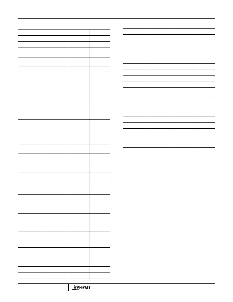
Electrical Specifications
V
S
= +5V, GND = 0V, T
A
= 25∞C, CE = +2V, unless otherwise specified.
PARAMETER
DESCRIPTION
CONDITIONS
MIN
TYP
MAX
UNIT
AC PERFORMANCE
d
G
Differential Gain Error (Note 1)
G = 2, R
L
= 150
to 2.5V, R
F
= 1k
0.1
%
d
P
Differential Phase Error (Note 1)
G = 2, R
L
= 150
to 2.5V, R
F
= 1k
0.1
∞
BW
Bandwidth
-3dB, G = 1, R
L
= 10k
,
R
F
= 0
100
MHz
-3dB, G = 1, R
L
= 150
,
R
F
= 0
60
MHz
BW1
Bandwidth
±0.1dB, G = 1, R
L
= 150
to GND, R
F
= 0
8
MHz
GBWP
Gain Bandwidth Product
60
MHz
SR
Slew Rate
G = 1, R
L
= 150
to GND, R
F
= 0, V
O
= 0.5V
to 3.5V
150
200
V/µs
t
S
Settling Time
to 0.1%, V
OUT
= 0V to 3V
35
ns
DC PERFORMANCE
A
VOL
Open Loop Voltage Gain
R
L
= no load, V
OUT
= 0.5V to 3V
54
65
dB
R
L
= 150
to GND, V
OUT
= 0.5V to 3V
40
50
dB
V
OS
Offset Voltage
V
CM
= 1V, SOT23-5 and MSOP packages
25
mV
V
CM
= 1V, All other packages
15
mV
T
C
V
OS
Input Offset Voltage Temperature
Coefficient
10
mV/∞C
I
B
Input Bias Current
V
CM
= 0V & 3.5V
2
100
nA
INPUT CHARACTERISTICS
CMIR
Common Mode Input Range
CMRR
47dB
0
3.5
V
CMRR
Common Mode Rejection Ratio
DC, V
CM
= 0 to 3.0V
50
60
dB
DC, V
CM
= 0 to 3.5V
47
60
dB
R
IN
Input Resistance
1.5
G
C
IN
Input Capacitance
1.5
pF
OUTPUT CHARACTERISTICS
V
OP
Positive Output Voltage Swing
R
L
= 150
to 2.5V (Note 2)
4.70
4.85
V
R
L
= 150
to GND (Note 2)
4.20
4.65
V
R
L
= 1k
to 2.5V (Note 2)
4.95
4.97
V
V
ON
Negative Output Voltage Swing
R
L
= 150
to 2.5V (Note 2)
0.15
0.30
V
R
L
= 150
to GND (Note 2)
0
V
R
L
= 1k
to 2.5V (Note 2)
0.03
0.05
V
+I
OUT
Positive Output Current
R
L
= 10
to 2.5V
60
90
120
mA
-I
OUT
Negative Output Current
R
L
= 10
to 2.5V
-50
-65
-80
mA
ENABLE (EL5146 & EL5246 ONLY)
EL5144, EL5146, EL5244, EL5246, EL5444

5
t
EN
Enable Time
EL5146, EL5246
500
ns
t
DIS
Disable Time
EL5146, EL5246
10
ns
I
IHCE
CE pin Input High Current
CE = 5V, EL5146, EL5246
0.003
1
mA
I
ILCE
CE pin Input Low Current
CE = 0V, EL5146, EL5246
-1.2
-3
mA
V
IHCE
CE pin Input High Voltage for Power
Up
EL5146, EL5246
2.0
V
V
ILCE
CE pin Input Low Voltage for Power
Down
EL5146, EL5246
0.8
V
SUPPLY
Is
ON
Supply Current - Enabled (per
amplifier)
No load, V
IN
= 0V, CE = 5V
7
8.8
mA
Is
OFF
Supply Current - Disabled (per
amplifier)
No load, V
IN
= 0V, CE = 0V
2.6
5
mA
PSOR
Power Supply Operating Range
4.75
5.0
5.25
V
PSRR
Power Supply Rejection Ratio
DC, V
S
= 4.75V to 5.25V
50
60
dB
NOTES:
1. Standard NTSC test, AC signal amplitude = 286mV
P-P
, f = 3.8MHz, V
OUT
is swept from 0.8V to 3.4V, R
L
is DC-coupled.
2. R
L
is total load resistance due to feedback resistor and load resistor.
Electrical Specifications
V
S
= +5V, GND = 0V, T
A
= 25∞C, CE = +2V, unless otherwise specified. (Continued)
PARAMETER
DESCRIPTION
CONDITIONS
MIN
TYP
MAX
UNIT
EL5144, EL5146, EL5244, EL5246, EL5444