Äîêóìåíòàöèÿ è îïèñàíèÿ www.docs.chipfind.ru
1
®
FN7188
CAUTION: These devices are sensitive to electrostatic discharge; follow proper IC Handling Procedures.
1-888-INTERSIL or 321-724-7143
|
Intersil (and design) is a registered trademark of Intersil Americas Inc.
Copyright © Intersil Americas Inc. 2003. All Rights Reserved. Elantec is a registered trademark of Elantec Semiconductor, Inc.
All other trademarks mentioned are the property of their respective owners.
EL5281
Dual 8ns High-Speed Comparator
The EL5281 comparator is designed
for operation in single supply and dual
supply applications with 5V to 12V
between V
S
+ and V
S
-. For single supplies, the inputs can
operate from 0.1V below ground for use in ground-sensing
applications.
The output side of the comparator can be supplied from a
single supply of 2.7V to 5V. The rail-to-rail output swing
enables direct connection of the comparator to both CMOS
and TTL logic circuits.
The latch input of the EL5281 can be used to hold the
comparator output value by applying a low logic level to the
pin. The EL5281 features two separate comparators.
The EL5281 is available in the 14-pin SO package and is
specified for operation over the full -40°C to +85°C
temperature range. Also available are a single (EL5181) and
quad versions (EL5481 and EL5482).
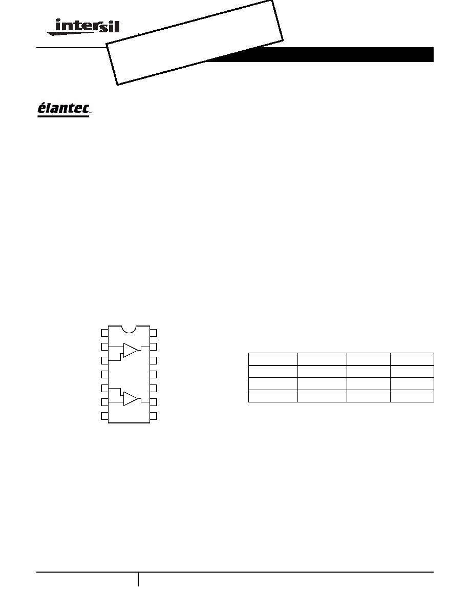
Pinout
Features
· 8ns Typ. Propagation Delay
· 5V to 12V Input Supply
· +2.7V to +5V Output Supply
· True-to-ground Input
· Rail-to-rail Outputs
· Active Low Latch
· Single Available (EL5181)
· Quad Available (EL5481 & EL5482)
· Pin-compatible 4ns Family Available (EL5x85, EL5287 &
EL5486)
Applications
· Threshold Detection
· High Speed Sampling Circuits
· High Speed Triggers
· Line Receivers
· PWM Circuits
· High Speed V/F Converters
1
2
3
4
14
13
12
11
5
6
7
10
9
8
EL5281
(14-PIN SO)
TOP VIEW
VS+
INA+
INA-
NC
INB+
INB-
VS-
VSD
OUTA
LATCHA
NC
LATCHB
OUTB
GND
+
-
+
-
Ordering Information
PART NUMBER
PACKAGE
TAPE & REEL
PKG. NO.
EL5281CS
14-Pin SO
-
MDP0027
EL5281CS-T7
14-Pin SO
7"
MDP0027
EL5281CS-T13
14-Pin SO
13"
MDP0027
Data Sheet
June 14, 2001
OBSO
LETE
PRO
DUCT
NO R
ECOM
MEN
DED
REPL
ACEM
ENT
conta
ct ou
r Tec
hnica
l Sup
port
Cent
er at
1-888
-INTE
RSIL
or w
ww.in
tersil
.com
/tsc
2
Absolute Maximum Ratings
(T
A
= 25°C)
Analog Supply Voltage (V
S
+ to V
S
-) . . . . . . . . . . . . . . . . . . . +12.6V
Digital Supply Voltage (V
SD
to GND) . . . . . . . . . . . . . . . . . . . . .+7V
Differential Input Voltage . . . . . . . . . . .[(V
S
-) -0.2V] to [(V
S
+) +0.2V]
Common-mode Input Voltage . . . . . . .[(V
S
-) -0.2V] to [(V
S
+) +0.2V]
Latch Input Voltage . . . . . . . . . . . . . . . . . . . . -0.2V to [(V
SD
)
+0.2V]
Storage Temperature Range . . . . . . . . . . . . . . . . . .-65°C to +150°C
Ambient Operating Temperature . . . . . . . . . . . . . . . .-40°C to +85°C
Operating Junction Temperature . . . . . . . . . . . . . . . . . . . . . . . 125°C
Power Dissipation . . . . . . . . . . . . . . . . . . . . . . . . . . . . . See Curves
CAUTION: Stresses above those listed in "Absolute Maximum Ratings" may cause permanent damage to the device. This is a stress only rating and operation of the
device at these or any other conditions above those indicated in the operational sections of this specification is not implied.
IMPORTANT NOTE: All parameters having Min/Max specifications are guaranteed. Typical values are for information purposes only. Unless otherwise noted, all tests
are at the specified temperature and are pulsed tests, therefore: T
J
= T
C
= T
A
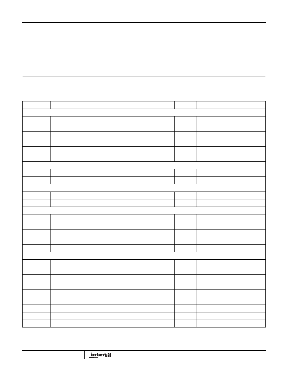
Electrical Specifications
V
S
= ±5V, V
SD
= 5V, R
L
= 2.3k
, C
L
= 15pF, T
A
= 25°C, unless otherwise specified.
PARAMETER
DESCRIPTION
CONDITION
MIN
TYP
MAX
UNIT
INPUT
V
OS
Input Offset Voltage
V
CM
= 0V, V
O
= 2.5V
1
4
mV
I
B
Input Bias Current
-6
-3.5
µA
C
IN
Input Capacitance
5
pF
I
OS
Input Offset Current
V
CM
= 0V, V
O
= 2.5V
-2.5
0.5
2.5
µA
V
CM
Input Voltage Range
(V
S
-) - 0.1
(V
S
+) - 2.25
V
CMRR
Common-mode Rejection Ratio
-5.1V < V
CM
< +2.75V
65
90
dB
OUTPUT
V
OH
Output High Voltage
V
IN
> 250mV
V
SD
- 0.6
V
SD
- 0.4
V
V
OL
Output Low Voltage
V
IN
> 250mV
GND + 0.25
GND + 0.5
V
DYNAMIC PERFORMANCE
t
PD
+
Positive Going Delay Time
V
IN
= 1V
P-P
, V
OD
= 50mV
8
12
ns
t
PD
-
Negative Going Delay Time
V
IN
= 1V
P-P
, V
OD
= 50mV
8
12
ns
SUPPLY
I
S
+
Positive Analog Supply Current
7
8.2
mA
I
S
-
Negative Analog Supply Current
5
6.5
mA
I
SD
Digital Supply Current
Output high
4
5
mA
Output low
0.75
1
mA
PSRR
Power Supply Rejection Ratio
60
80
dB
LATCH
V
LH
Latch Input Voltage High
2.0
V
V
LL
Latch Input Voltage Low
0.8
V
I
LH
Latch Input Current High
V
LH
= 3.0V
-30
-18
µA
I
LL
Latch Input Current Low
V
LL
= 0.3V
-30
-24
µA
t
D
+
Latch Disable to High Delay
6
ns
t
D
-
Latch Disable to Low Delay
6
ns
t
S
Minimum Setup Time
2
ns
t
H
Minimum Hold Time
1
ns
t
PW
(D)
Minimum Latch Disable Pulse Width
10
ns
EL5281
3
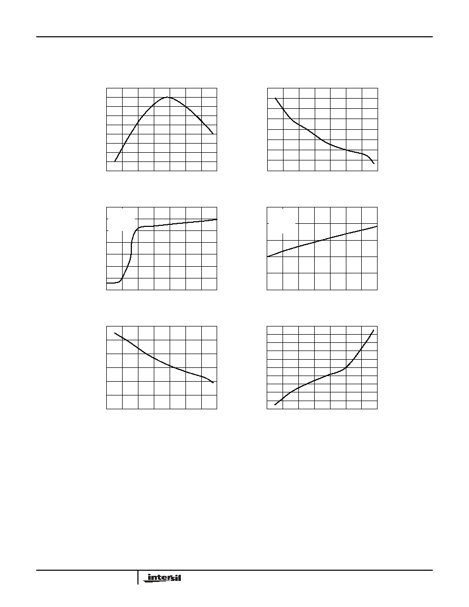
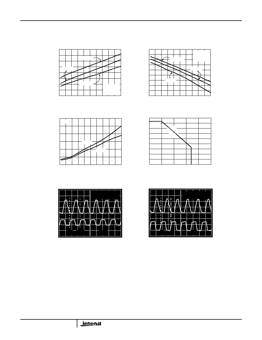
Typical Performance Curves
Positive Supply Current vs Temperature
7.15
7.1
7.05
7
6.95
6.9
6.85
6.8
6.75
6.7
-50
-30
-10
10
30
50
70
90
Temperature (°C)
I
S
+ (
m
A
)
Negative Supply Current vs Temperature
-4.4
-4.5
-4.6
-4.7
-4.8
-4.9
-5
-5.1
-5.2
-50
-30
-10
10
30
50
70
90
Temperature (°C)
I
S
- (
m
A
)
Input Bias Current vs Temperature
6
5
4
3
2
1
0
-50
-30
-10
10
30
50
70
90
Temperature (°C)
IB
(
µ
A
)
Offset Voltage vs Temperature
0.7
0.6
0.4
0.3
0.2
0.1
0
-0.1
-0.2
-0.3
-50
-30
-10
10
30
50
70
90
Temperature (°C)
V
OS
(m
V)
0.5
Negative Supply Current vs Negative Supply
Voltage
5.5
3
5
3.5
4.5
4
0
7
1
2
3
4
5
6
V
S
- (V)
I
S
- (mA)
7
0
5
1
3
2
I
S
+ (
m
A
)
Positive Supply Current vs Supply Voltage
0
7
1
2
3
4
5
6
V
S
+ (V)
6
4
V
S
-=-5V
V
SD
=5V
V
IN
=50mV
T
A
=25°C
V
S
+=5V
V
SD
=5V
V
IN
=50mV
T
A
=25°C
EL5281
4
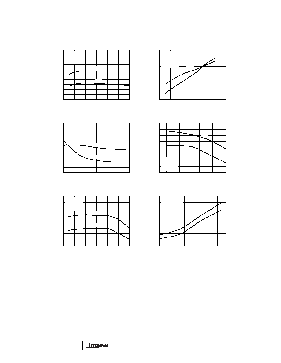
Typical Performance Curves
(Continued)
Propagation Delay vs Supply Voltage
10
9.5
8.5
7.5
7
6.5
6
5.5
5
9
8
4
4.5
5
5.5
6
±V
S
(V)
D
e
l
ay Time (ns
)
T
PD
+
T
PD
-
V
SD
=V
S
+
V
IN
=1V Step
V
OD
=50mV
R
L
=2.2k
Propagation Delay vs Overdrive
10
9.5
8.5
8
7.5
7
6.5
6
9
0
0.2
0.6
1
1.2
1.6
2
V
OD
(V)
D
e
l
ay Time (ns
)
T
PD
+
T
PD
-
V
S
=±5V
V
SD
=5V
V
IN
=3V Step
R
L
=2.2k
0.4
0.8
1.4
1.8
Propagation Delay vs Overdrive
11
10.5
9.5
9
8.5
8
7.5
7
10
0
0.5
1
2
3
V
OD
(V)
D
e
la
y Tim
e
(
n
s)
T
PD
+
T
PD
-
V
S
=±5V
V
SD
=5V
R
L
=2.2k
V
IN
=5V Step
1.5
2.5
Propagation Delay vs Source Resistance
20
18
14
12
10
8
6
4
16
0
0.2
0.4
1
1.6
Source Resistance (k
)
D
e
la
y Tim
e
(
n
s)
T
PD
+
T
PD
-
0.6
1.4
1.2
0.8
V
S
=±5V
V
SD
=5V
R
L
=2.2k
V
IN
=1V Step
V
OD
=50mV
Propagation Delay vs Overdrive
10
9.5
8.5
7.5
7
6.5
6
5.5
5
9
8
0
100
200
300
400
500
600
V
OD
(mV)
D
e
lay
Time
(
n
s)
T
PD
+
T
PD
-
V
S
=±5V
V
SD
=5V
V
IN
=1V Step
R
L
=2.2k
Propagation Delay vs Load Capacitance
12
10
9
8
7
6
11
0
20
40
60
80
100
120
C
LOAD
(pF)
D
e
lay
Time
(
n
s)
T
PD
+
T
PD
-
V
S
=±5V
V
SD
=5V
R
L
=2.2k
V
IN
=1V Step
V
OD
=50mV
EL5281
5
Typical Performance Curves
(Continued)
0
10
2
4
6
Load Current (mA)
Output Low Voltage vs Load Current
0.31
0.15
0.27
Outp
ut Low
Voltage
(V)
8
0.23
0.19
V
S
=±5V
V
SD
=5V
V
IN
=-50mV
0
10
2
4
6
Load Current (mA)
8
Output High Voltage vs Load Current
4.75
4.3
4.7
Out
p
u
t
High
Volt
age
(V
)
4.65
4.6
4.55
4.5
4.45
4.4
4.35
V
S
=±5V
V
SD
=5V
V
IN
=50mV
Package Power Dissipation vs Ambient Temp.
JEDEC JESD51-3 Low Effective Thermal Conductivity
Test Board
0.9
0
0.6
0.3
0.2
0.1
Powe
r Dis
s
ipa
t
i
o
n
(W
)
0.8
0.4
0
100
75
50
25
Ambient Temperature (°C)
125
2V
V
IN
=1V
P-P
F
IN
=30MH
1V
20ns
V
S
=±5V
V
SD
=5V
Output with 30MHz Input
V
IN
=1V
P-P
2V
2V
20ns
V
IN
=3V
P-P
F
IN
=30MHz
V
S
=±5V
V
SD
=5V
Output with 30MHz Input
V
IN
=3V
P-P
V
O
V
IN
V
O
V
IN
0.5
0.7
85
833mW
SO
14
120
°C
/W
T
A
=-40°C
T
A
=85°C
T
A
=25°C
T
A
=-40°C
T
A
=85°C
T
A
=25°C
Digital Supply Current vs Input Switching
Frequency
30
0
25
15
10
5
I
SD
(m
A)
20
0
45
35
25
15
5
Frequency (MHz)
50
40
30
20
10
V
SD
=5V
V
SD
=3V
VS=±5V
EL5281