1
®
FN7357.3
CAUTION: These devices are sensitive to electrostatic discharge; follow proper IC Handling Procedures.
1-888-INTERSIL or 321-724-7143
|
Intersil (and design) is a registered trademark of Intersil Americas Inc.
Copyright © Intersil Americas Inc. 2002-2004. All Rights Reserved. Elantec is a registered trademark of Elantec Semiconductor, Inc.
All other trademarks mentioned are the property of their respective owners.
EL5106, EL5306
350MHz Fixed Gain Amplifiers with Enable
The EL5106 and EL5306 are fixed gain amplifiers with a
bandwidth of 350MHz. This makes these amplifiers ideal for
today's high speed video and monitor applications. They
feature internal gain setting resistors and can be configured
in a gain of +1, -1 or +2.
With a supply current of just 1.5mA and the ability to run
from a single supply voltage from 5V to 12V, these amplifiers
are also ideal for handheld, portable or battery powered
equipment.
The EL5106 and EL5306 also incorporate an enable and
disable function to reduce the supply current to 25µA typical
per amplifier. Allowing the CE pin to float or applying a low
logic level will enable the amplifier.
The EL5106 is offered in the 6-pin SOT-23 and the industry-
standard 8-pin SO packages and the EL5306 is available in
the 16-pin SO and 16-pin QSOP packages. All operate over
the industrial temperature range of -40°C to +85°C.
Features
· Pb-free Available as an Option
· Gain selectable (+1, -1, +2)
· 350MHz -3dB BW (A
V
= 2)
· 1.5mA supply current per amplifier
· Fast enable/disable
· Single and dual supply operation, from 5V to 12V
· Available in SOT-23 packages
· 450MHz, 3.5mA product available (EL5108 & EL5308)
Applications
· Battery powered equipment
· Handheld, portable devices
· Video amplifiers
· Cable drivers
· RGB amplifiers
Ordering Information
PART
NUMBER
PACKAGE
TAPE &
REEL
PKG. DWG. #
EL5106IW-T7
6-Pin SOT-23
7" (3K pcs)
MDP0038
EL5106IW-T7A
6-Pin SOT-23
7" (250 pcs)
MDP0038
EL5106IS
8-Pin SO
-
MDP0027
EL5106IS-T7
8-Pin SO
7"
MDP0027
EL5106IS-T13
8-Pin SO
13"
MDP0027
EL5306IS
16-Pin SO (0.150")
-
MDP0027
EL5306IS-T7
16-Pin SO (0.150")
7"
MDP0027
EL5306IS-T13
16-Pin SO (0.150")
13"
MDP0027
EL5306IU
16-Pin QSOP
-
MDP0040
EL5306IU-T7
16-Pin QSOP
7"
MDP0040
EL5306IU-T13
16-Pin QSOP
13"
MDP0040
EL5306IUZ
(See Note)
16-Pin QSOP
(Pb-free)
-
MDP0040
EL5306IUZ-T7
(See Note)
16-Pin QSOP
(Pb-free)
7"
MDP0040
EL5306IUZ-
T13 (See Note)
16-Pin QSOP
(Pb-free)
13"
MDP0040
NOTE: Intersil Pb-free products employ special Pb-free material
sets; molding compounds/die attach materials and 100% matte tin
plate termination finish, which is compatible with both SnPb and
Pb-free soldering operations. Intersil Pb-free products are MSL
classified at Pb-free peak reflow temperatures that meet or exceed
the Pb-free requirements of IPC/JEDEC J Std-020B.
Data Sheet
September 1, 2004
3
Absolute Maximum Ratings
(T
A
= 25°C)
Supply Voltage between V
S
+ and V
S
- . . . . . . . . . . . . . . . . . . . 13.2V
Maximum Continuous Output Current . . . . . . . . . . . . . . . . . . . 50mA
Operating Junction Temperature . . . . . . . . . . . . . . . . . . . . . . . 125°C
Power Dissipation . . . . . . . . . . . . . . . . . . . . . . . . . . . . . See Curves
Pin Voltages. . . . . . . . . . . . . . . . . . . . . . . . . V
S
- -0.5V to V
S
+ +0.5V
Storage Temperature . . . . . . . . . . . . . . . . . . . . . . . .-65°C to +150°C
Ambient Operating Temperature . . . . . . . . . . . . . . . .-40°C to +85°C
CAUTION: Stresses above those listed in "Absolute Maximum Ratings" may cause permanent damage to the device. This is a stress only rating and operation of the
device at these or any other conditions above those indicated in the operational sections of this specification is not implied.
IMPORTANT NOTE: All parameters having Min/Max specifications are guaranteed. Typical values are for information purposes only. Unless otherwise noted, all tests
are at the specified temperature and are pulsed tests, therefore: T
J
= T
C
= T
A
Electrical Specifications
V
S
+ = +5V, V
S
- = -5V, R
L
= 150
, T
A
= 25°C unless otherwise specified.
PARAMETER
DESCRIPTION
CONDITIONS
MIN
TYP
MAX
UNIT
AC PERFORMANCE
BW
-3dB Bandwidth
A
V
= +1
250
MHz
A
V
= -1
380
MHz
A
V
= +2
350
MHz
BW1
0.1dB Bandwidth
20
MHz
SR
Slew Rate
V
O
= -2.5V to +2.5V, A
V
= +2
3000
4500
V/µs
t
S
0.1% Settling Time
V
OUT
= -2.5V to +2.5V, A
V
= 2
16
ns
e
N
Input Voltage Noise
2.8
nV/
Hz
i
N
+
IN+ Input Current Noise
6
pA/
Hz
dG
Differential Gain Error (Note 1)
A
V
= +2
0.02
%
dP
Differential Phase Error (Note 1)
A
V
= +2
0.04
°
DC PERFORMANCE
V
OS
Offset Voltage
-10
1
10
mV
T
C
V
OS
Input Offset Voltage Temperature
Coefficient
Measured from T
MIN
to T
MAX
5
µV/°C
A
E
Gain Error
V
O
= -3V to +3V, R
L
= 150
1
2.5
%
R
F
, R
G
Internal R
F
and R
G
325
INPUT CHARACTERISTICS
CMIR
Common Mode Input Range
±3
±3.3
V
+I
IN
+ Input Current
1.5
7
µA
R
IN
Input Resistance
at I
N
+
2
M
C
IN
Input Capacitance
1
pF
OUTPUT CHARACTERISTICS
V
O
Output Voltage Swing
R
L
= 150
to GND
±3.4
±3.6
V
R
L
= 1k
to GND
±3.7
±3.85
V
I
OUT
Output Current
R
L
= 10
to GND
60
100
mA
SUPPLY
I
SON
Supply Current - Enabled (per amplifier)
No load, V
IN
= 0V
1.35
1.5
1.82
mA
I
SOFF
Supply Current - Disabled (per amplifier) No load, V
IN
= 0V
12
25
µA
PSRR
Power Supply Rejection Ratio
DC, V
S
= ±4.75V to ±5.25V
75
dB
ENABLE
t
EN
Enable Time
280
ns
EL5106, EL5306
4
t
DIS
Disable Time
400
ns
I
IHCE
CE Pin Input High Current
CE = V
S
+
1
5
25
µA
I
ILCE
CE Pin Input Low Current
CE = V
S
-
+1
0
-1
µA
V
IHCE
CE Input High Voltage for Power-down
V
S
+ -1
V
V
ILCE
CE Input Low Voltage for Enable
V
S
+ -3
V
NOTE:
1. Standard NTSC test, AC signal amplitude = 286mV
P-P
, f = 3.58MHz
Electrical Specifications
V
S
+ = +5V, V
S
- = -5V, R
L
= 150
, T
A
= 25°C unless otherwise specified. (Continued)
PARAMETER
DESCRIPTION
CONDITIONS
MIN
TYP
MAX
UNIT
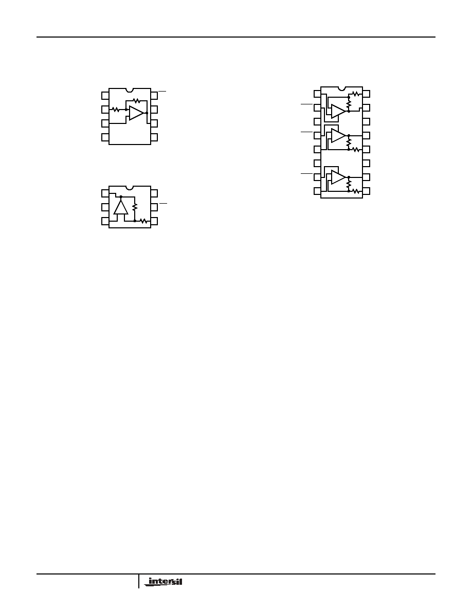
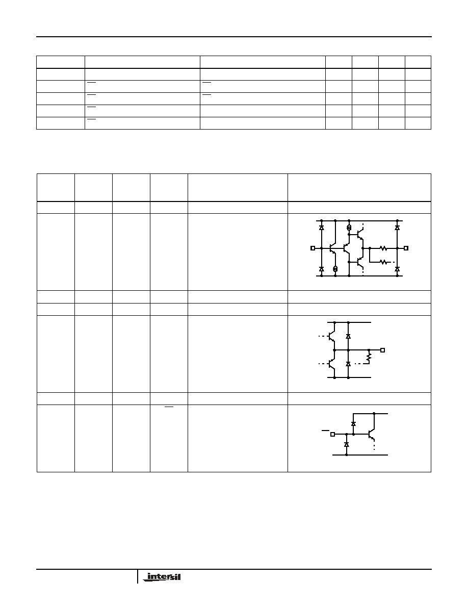
Pin Descriptions
EL5106
(SO8)
EL5106
(SOT23-6)
EL5306
(SO16,
QSOP16)
PIN
NAME
FUNCTION
EQUIVALENT CIRCUIT
1, 5
6, 11
NC
Not connected
2
4
9, 12, 16
IN-
Inverting input
CIRCUIT 1
3
3
1, 5, 8
IN+
Non-inverting input
(Reference Circuit 1)
4
2
3
VS-
Negative supply
6
1
10, 13, 15
OUT
Output
CIRCUIT 2
7
6
14
VS+
Positive supply
8
5
2, 4, 7
CE
Chip enable
CIRCUIT 3
R
G
R
F
IN-
IN+
R
F
OUT
V
S
+
V
S
-
CE
EL5106, EL5306
5
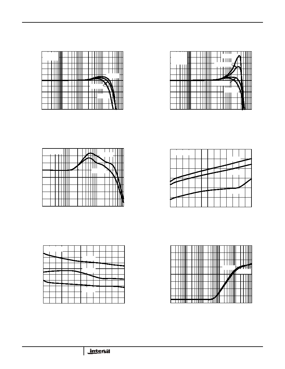
Typical Performance Curves
FIGURE 1. FREQUENCY RESPONSE
FIGURE 2. FREQUENCY RESPONSE FOR VARIOUS C
L
FIGURE 3. GROUP DELAY vs FREQUENCY
FIGURE 4. BANDWIDTH vs SUPPLY VOLTAGE
FIGURE 5. PEAKING vs SUPPLY VOLTAGE
FIGURE 6. POWER SUPPLY REJECTION RATIO vs
FREQUENCY
100K
FREQUENCY (Hz)
1M
10M
1G
N
O
RM
AL
IZE
D
G
A
IN
(
d
B)
1
-1
-3
-5
3
5
100M
A
V
= -1
A
V
= 1
A
V
= 2
V
S
=±5V
R
L
=150
100K
FREQUENCY (Hz)
1M
10M
1G
G
A
IN (
d
B
)
7
5
3
1
9
11
100M
C
L
= 10pF
C
L
= 6.8pF
C
L
= 2.2pF
C
L
= 0pF
A
V
=+2
V
S
=±5V
R
L
=150
1
FREQUENCY (Hz)
10
100
1K
DE
L
A
Y TIME
(
n
s
)
0.8
0.4
0
1.2
1.6
A
V
= 1, 2
A
V
= -1
R
L
= 150
4.5
FREQUENCY (Hz)
5
5.5
11
BW (MHz
)
250
150
350
450
6
7
7.5
8
8.5
9
9.5 10 10.5
6.5
A
V
= -1
A
V
= 2
A
V
= 1
R
L
= 150
4.5
V
S
(V)
5
5.5
11
PEAKING (dB
)
0.2
0
0.4
0.6
0.8
1
6
7
7.5
8
8.5
9
9.5 10 10.5
6.5
A
V
= 1
A
V
= 2
R
L
= 150
A
V
= -1
1K
FREQUENCY (Hz)
10K
100M
P
S
RR (dB)
-80
-60
-40
-20
0
100K
1M
10M
PSRR+
-10
-30
-50
-70
PSRR-
P
S
RR (dB)
EL5106, EL5306