 | ÐлекÑÑоннÑй компоненÑ: EL5325A | СкаÑаÑÑ:  PDF PDF  ZIP ZIP |
Äîêóìåíòàöèÿ è îïèñàíèÿ www.docs.chipfind.ru
1
®
FN7447
EL5325A
12-Channel TFT-LCD Reference Voltage
Generator with External Shutdown
The EL5325A with external shutdown
is designed to produce the reference
voltages required in TFT-LCD
applications. Each output is programmed to the required
voltage with 10 bits of resolution. Reference pins determine
the high and low voltages of the output range, which are
capable of swinging to either supply rail. Programming of
each output is performed using the 3-wire, SPI compatible
interface.
A number of EL5325A can be stacked for applications
requiring more than 12 outputs. The reference inputs can be
tied to the rails, enabling each part to output the full voltage
range, or alternatively, they can be connected to external
resistors to split the output range and enable finer
resolutions of the outputs.
The EL5325A has 12 outputs and is available in a 28-pin
TSSOP package. They are specified for operation over the
full -40°C to +85°C temperature range.
Features
· 12-channel reference outputs
· Accuracy of ±1%
· Supply voltage of 5V to 16.5V
· Digital supply 3.3V to 5V
· Low supply current of 10mA
· Rail-to-rail capability
· Internal thermal protection
· External shutdown
· Pb-free available
Applications
· TFT-LCD drive circuits
· Reference voltage generators
Ordering Information
PART
NUMBER
PACKAGE
TAPE &
REEL
PKG.
DWG. #
EL5325AIRZ
(Note)
28-Pin TSSOP
(Pb-Free)
-
MDP0044
EL5325AIRZ-T7
(Note)
28-Pin TSSOP
(Pb-Free)
7"
MDP0044
EL5325AIRZ-T13
(Note)
28-Pin TSSOP
(Pb-Free)
13"
MDP0044
NOTE: Intersil Pb-Free products employ special Pb-free material
sets; molding compounds/die attach materials and 100% matte tin
plate termination finish, which is compatible with both SnPb and Pb-
free soldering operations. Intersil Pb-Free products are MSL
classified at Pb-free peak reflow temperatures that meet or exceed
the Pb-free requirements of IPC/JEDEC J Std-020B.
Pinout
EL5325A
(28-PIN TSSOP)
TOP VIEW
ENA
OUTA
SDI
SCLK
SDO
EXT_OSC
VS
SHDN
VSD
REFH
REFL
VS
GND
CAP
NC
OUTB
OUTC
GND
OUTD
OUTE
OUTF
OUTG
OUTH
OUTI
GND
OUTJ
OUTK
OUTL
1
2
3
4
28
27
26
25
5
6
7
24
23
22
8
21
9
10
20
19
11
12
13
18
17
16
14
15
Data Sheet
April 28, 2004
CAUTION: These devices are sensitive to electrostatic discharge; follow proper IC Handling Procedures.
1-888-INTERSIL or 321-724-7143
|
Intersil (and design) is a registered trademark of Intersil Americas Inc.
Copyright © Intersil Americas Inc. 2004. All Rights Reserved. Elantec is a registered trademark of Elantec Semiconductor, Inc.
All other trademarks mentioned are the property of their respective owners.
2
IMPORTANT NOTE: All parameters having Min/Max specifications are guaranteed. Typ values are for information purposes only. Unless otherwise noted, all tests are
at the specified temperature and are pulsed tests, therefore: T
J
= T
C
= T
A
Absolute Maximum Ratings
(T
A
= 25°C)
Supply Voltage between V
S
& GND . . . . . . 4.5V (min) to 18V (max)
Supply Voltage between V
SD
& GND . 3V (min) to V
S
and 7V (max)
Maximum Continuous Output Current . . . . . . . . . . . . . . . . . . . 30mA
Power Dissipation . . . . . . . . . . . . . . . . . . . . . . . . . . . . . See Curves
Maximum Die Temperature . . . . . . . . . . . . . . . . . . . . . . . . . . +125°C
Storage Temperature . . . . . . . . . . . . . . . . . . . . . . . .-65°C to +150°C
Ambient Operating Temperature . . . . . . . . . . . . . . . .-40°C to +85°C
CAUTION: Stresses above those listed in "Absolute Maximum Ratings" may cause permanent damage to the device. This is a stress only rating and operation of the
device at these or any other conditions above those indicated in the operational sections of this specification is not implied.
Electrical Specifications
V
S
= 15V, V
SD
= 5V, V
REFH
= 13V, V
REFL
= 2V, R
L
= 1.5k
and C
L
= 200pF to 0V, T
A
= 25°C, unless otherwise
specified.
PARAMETER
DESCRIPTION
CONDITIONS
MIN
TYP
MAX
UNIT
SUPPLY
I
S
Supply Current
No load
10.2
12.5
mA
I
SD
Digital Supply Current
0.17
0.35
mA
ANALOG
V
OL
Output Swing Low
Sinking 5mA (V
REFH
= 15V, V
REFL
= 0)
50
150
mV
V
OH
Output Swing High
Sourcing 5mA (V
REFH
= 15V, V
REFL
= 0)
14.85
14.95
V
I
SC
Short Circuit Current
R
L
= 10
100
140
mA
PSRR
Power Supply Rejection Ratio
V
S
+ is moved from 14V to 16V
45
65
dB
t
D
Program to Out Delay
4
ms
V
AC
Accuracy referred to the ideal value
Code = 512
20
mV
V
MIS
Channel to Channel Mismatch
Code = 512
2
mV
V
DROOP
Droop Voltage
1
2
mV/ms
R
INH
Input Resistance @ V
REFH
, V
REFL
32
k
REG
Load Regulation
I
OUT
= 5mA step
0.5
1.5
mV/mA
CAP
Band Gap
By pass with 0.1µF
1
1.3
1.6
V
DIGITAL
V
IH
Logic 1 Input Voltage
V
SD
= 5V
4
V
V
SD
= 3.3V
2
V
F
CLK
Clock Frequency
5
MHz
V
IL
Logic 0 Input Voltage
V
SD
= 3.3V/5V
1
V
t
S
Setup Time
20
ns
t
H
Hold Time
20
ns
t
LC
Load to Clock Time
20
ns
t
CE
Clock to Load Line
20
ns
t
DCO
Clock to Out Delay Time
Negative edge of SCLK
10
ns
R
SDIN
S
DIN
Input Resistance
1
G
T
PULSE
Minimum Pulse Width for EXT_OSC Signal
5
µs
Duty Cycle
Duty Cycle for EXT_OSC Signal
50
%
INL
Integral Nonlinearity Error
1.3
LSB
DNL
Differential Nonlinearity Error
0.5
LSB
F_OSC
Internal Refresh Oscillator Frequency
OSC_Select = 0
21
kHz
V
IH_SHDN
SHDN Voltage Input High
2
V
I
IH_SHDN
SHDN Current Input High
SHDN = 2V
100
µA
EL5325A
3
Pin Descriptions
EL5325A
PIN NAME
PIN TYPE
PIN FUNCTION
1
ENA
Logic Input
Chip select, low enables data input to logic
2
SDI
Logic Input
Serial data input
3
SCLK
Logic Input
Serial data clock
4
SDO
Logic Output
Serial data output
5
EXT_OSC
Logic Input/Output
External oscillator input or internal oscillator output
6, 11
VS+
Analog Power
Positive supply voltage for analog circuits
7
SHDN
Logic Input
Chip shutdown: float enables chip, high > 2V disables chip
8
VSD
Digital Power
Positive power supply for digital circuits (3.3V - 5V)
9
REFH
Analog Reference Input
High reference voltage
10
REFL
Analog Reference Input
Low reference voltage
12
GND
Ground
Ground
13
CAP
Analog Bypass Pin
Decoupling capacitor for internal reference generator, 0.1µF
14
NC
Not connected
17
OUTJ
Analog Output
Channel J programmable output voltage
19
OUTI
Analog Output
Channel I programmable output voltage
20
OUTH
Analog Output
Channel H programmable output voltage
21
OUTG
Analog Output
Channel G programmable output voltage
22
OUTF
Analog Output
Channel F programmable output voltage
23
OUTE
Analog Output
Channel E programmable output voltage
24
OUTD
Analog Output
Channel D programmable output voltage
26
OUTC
Analog Output
Channel C programmable output voltage
27
OUTB
Analog Output
Channel B programmable output voltage
28
OUTA
Analog Output
Channel A programmable output voltage
15
OUTL
Analog Output
Channel L programmable output voltage
16
OUTK
Analog Output
Channel K programmable output voltage
18, 25
GND
Power
Ground
EL5325A
4
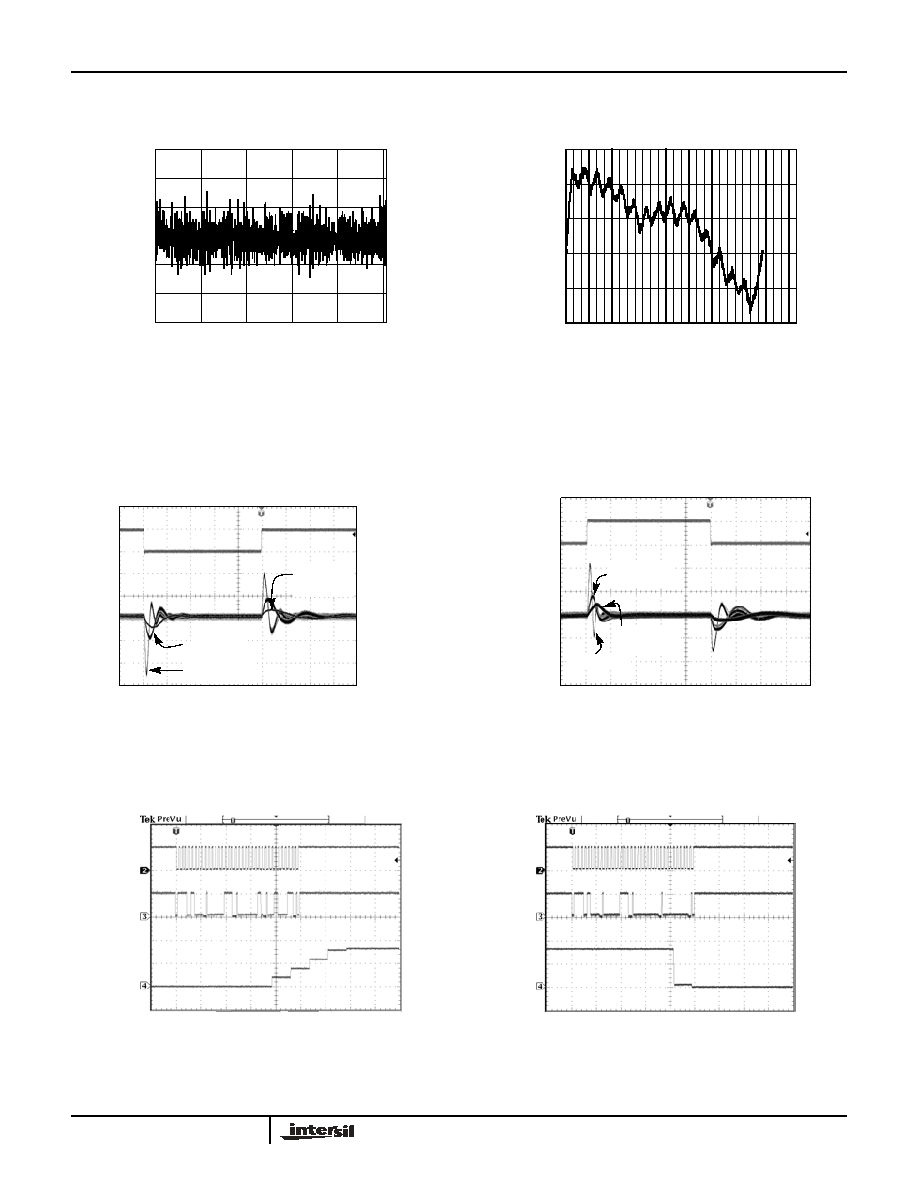
Typical Performance Curves
FIGURE 1. DIFFERENTIAL NONLINEARITY vs CODE
FIGURE 2. INTEGRAL NONLINEARITY ERROR
FIGURE 3. TRANSIENT LOAD REGULATION (SOURCING)
FIGURE 4. TRANSIENT LOAD REGULATION (SINKING)
FIGURE 5. LARGE SIGNAL RESPONSE (RISING FROM 0V
TO 8V)
FIGURE 6. LARGE SIGNAL RESPONSE (FALLING FROM 8V
TO 0V)
0.3
0.2
0.1
0
-0.1
-0.2
-0.3
10
210
410
610
810
1010
INPUT CODE
DIFFERENTIA
L NONL
IN
E
ARITY (LSB)
V
S
=15V, V
SD
=5V, V
REFH
=13V, V
REFL
=2V
-1
-0.5
0
0.5
1
1.5
0
200
400
600
800
1000
1200
CODE
INL
(
L
S
B
)
REFH=13V, REFL=2V
0mA
5V
5mA/DIV
200mV/DIV
5mA
C
L
=180pF
C
L
=4.7nF
R
S
=20
C
L
=1nF
R
S
=20
V
S
=V
REFH
=15V
M=400ns/DIV
5mA
0mA
C
L
=1nF
R
S
=20
C
L
=180pF
V
S
=V
REFH
=15V
M=400ns/DIV
C
L
=4.7nF
R
S
=20
5V
SDA
0V
OUTPUT
SCLK
0V
5V
0V
10V
5V
M=400µs/DIV
SDA
OUTPUT
SCLK
M=400µs/DIV
EL5325A
5
General Description
The EL5325A provides a versatile method of providing the
reference voltages that are used in setting the transfer
characteristics of LCD display panels. The V/T
(Voltage/Transmission) curve of the LCD panel requires that
a correction is applied to make it linear; however, if the panel
is to be used in more than one application, the final curve
may differ for different applications. By using the EL5325A,
the V/T curve can be changed to optimize its characteristics
according to the required application of the display product.
Each of the eight reference voltage outputs can be set with a
10-bit resolution. These outputs can be driven to within
50mV of the power rails of the EL5325A. As all of the output
buffers are identical, it is also possible to use the EL5325A
for applications other than LCDs where multiple voltage
references are required that can be set to 10 bit accuracy.
Digital Interface
The EL5325A uses a simple 3-wire SPI compliant digital
interface to program the outputs. The EL5325A can support
the clock rate up to 5MHz.
Serial Interface
The EL5325A is programmed through a three-wire serial
interface. The start and stop conditions are defined by the
ENA signal. While the ENA is low, the data on the SDI (serial
data input) pin is shifted into the 16-bit shift register on the
positive edge of the SCLK (serial clock) signal. The MSB (bit
15) is loaded first and the LSB (bit 0) is loaded last (see
Table 1). After the full 16-bit data has been loaded, the ENA
is pulled high and the addressed output channel is updated.
The SCLK is disabled internally when the ENA is high. The
SCLK must be low before the ENA is pulled low.
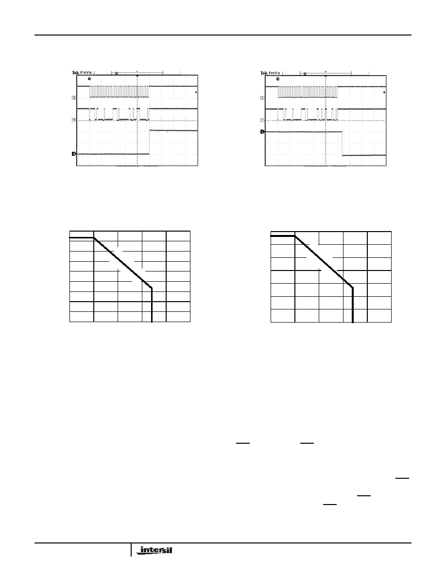
FIGURE 7. SMALL SIGNAL RESPONSE (RISING FROM 0V
TO 200mV)
FIGURE 8. SMALL SIGNAL RESPONSE (FALLING FROM
200mV TO 0V)
FIGURE 9. POWER DISSIPATION vs AMBIENT
TEMPERATURE
FIGURE 10. POWER DISSIPATION vs AMBIENT
TEMPERATURE
Typical Performance Curves
(Continued)
SDA
OUTPUT
SCLK
M=400µs/DIV
5V
0V
0V
5V
0V
200mV
SDA
OUTPUT
SCLK
M=400µs/DIV
833mW
JEDEC JESD51-3 LOW EFFECTIVE THERMAL
CONDUCTIVITY TEST BOARD
0.9
0.8
0.6
0.4
0.3
0.2
0.1
0
0
25
50
75
100
125
AMBIENT TEMPERATURE (°C)
POWER DISS
IP
A
T
ION
(W)
85
0.7
0.5
JA
=12
0°C
/W
TS
SO
P2
8
1.333W
JEDEC JESD51-7 HIGH EFFECTIVE THERMAL
CONDUCTIVITY TEST BOARD
1.4
1.2
1
0.8
0.6
0.4
0.2
0
0
25
50
75
100
125
AMBIENT TEMPERATURE (°C)
PO
WER D
I
SS
IP
A
T
IO
N
(W)
85
JA
=7
5°C
/W
TS
SO
P2
8
EL5325A