Äîêóìåíòàöèÿ è îïèñàíèÿ www.docs.chipfind.ru
1
®
FN7118.3
EL5226, EL5326
10- and 12-Channel TFT-LCD Reference
Voltage Generators
The EL5226 and EL5326 are designed to produce the
reference voltages required in TFT-LCD applications. Each
output is programmed to the required voltage with 10 bits of
resolution. Reference pins determine the high and low
voltages of the output range, which are capable of swinging
to either supply rail. Programming of each output is
performed using the I
2
C serial interface.
A number of the EL5226 and EL5326 can be stacked for
applications requiring more than 12 outputs. The reference
inputs can be tied to the rails, enabling each part to output
the full voltage range, or alternatively, they can be connected
to external resistors to split the output range and enable finer
resolutions of the outputs.
The EL5226 has 10 outputs and the EL5326 has 12 outputs
and both are available in a 28-pin TSSOP package. They
are specified for operation over the full -40°C to +85°C
temperature range.
Features
· 10- to 12-channel reference outputs
· Accuracy of ±1%
· Supply voltage of 5V to 16.5V
· Digital supply 3.3V to 5V
· Low supply current of 10mA
· Rail-to-rail capability
· Pb-Free available (RoHS compliant)
Applications
· TFT-LCD drive circuits
· Reference voltage generators
Ordering Information
PART
NUMBER
PACKAGE
TAPE & REEL PKG. DWG. #
EL5226IR
28-Pin TSSOP
-
MDP0044
EL5226IR-T7
28-Pin TSSOP
7"
MDP0044
EL5226IR-T13
28-Pin TSSOP
13"
MDP0044
EL5226IRZ
(See Note)
28-Pin TSSOP
(Pb-free)
-
MDP0044
EL5226IRZ-T7
(See Note)
28-Pin TSSOP
(Pb-free)
7"
MDP0044
EL5226IRZ-T13
(See Note)
28-Pin TSSOP
(Pb-free)
13"
MDP0044
EL5326IR
28-Pin TSSOP
-
MDP0044
EL5326IR-T7
28-Pin TSSOP
7"
MDP0044
EL5326IR-T13
28-Pin TSSOP
13"
MDP0044
EL5326IRZ
(See Note)
28-Pin TSSOP
(Pb-free)
-
MDP0044
EL5326IRZ-T7
(See Note)
28-Pin TSSOP
(Pb-free)
7"
MDP0044
EL5326IRZ-T13
(See Note)
28-Pin TSSOP
(Pb-free)
13"
MDP0044
NOTE: Intersil Pb-free products employ special Pb-free material sets;
molding compounds/die attach materials and 100% matte tin plate
termination finish, which are RoHS compliant and compatible with
both SnPb and Pb-free soldering operations. Intersil Pb-free products
are MSL classified at Pb-free peak reflow temperatures that meet or
exceed the Pb-free requirements of IPC/JEDEC J STD-020.
Data Sheet
May 9, 2005
CAUTION: These devices are sensitive to electrostatic discharge; follow proper IC Handling Procedures.
1-888-INTERSIL or 1-888-352-6832
|
Intersil (and design) is a registered trademark of Intersil Americas Inc.
Copyright Intersil Americas Inc. 2003, 2004, 2005. All Rights Reserved
All other trademarks mentioned are the property of their respective owners.
2
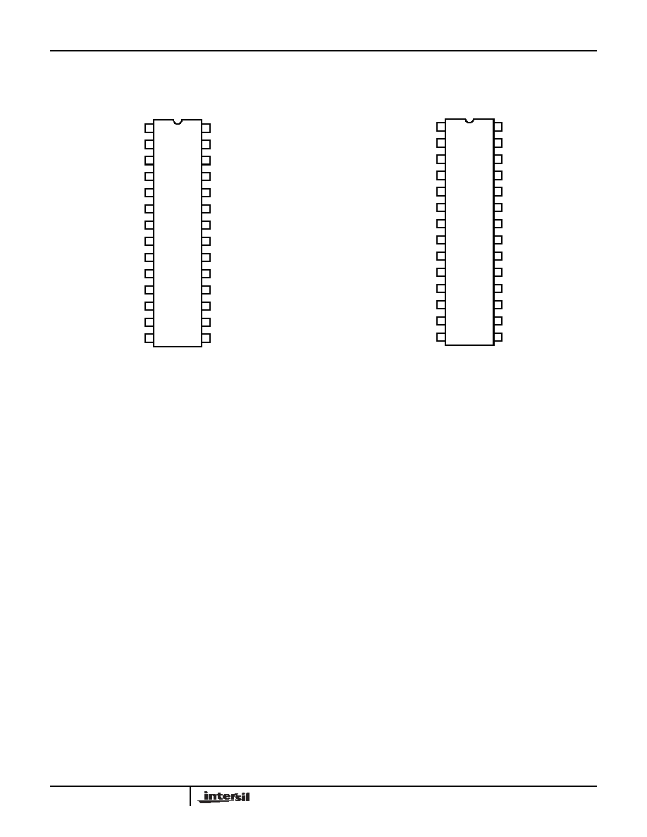
Pinouts
EL5226
(28-PIN TSSOP)
TOP VIEW
EL5326
(28-PIN TSSOP)
TOP VIEW
STD_REG
NC
SCL
SDA
OSC
OSC_SELECT
VS
NC
VSD
REFH
REFL
VS
GND
CAP
DEV_ADDRO
OUTA
OUTB
OUTC
GND
OUTD
OUTE
OUTF
OUTG
GND
OUTH
OUTI
OUTJ
NC
1
2
3
4
28
27
26
25
5
6
7
24
23
22
8
21
9
10
20
19
11
12
13
18
17
16
14
15
STD_REG
OUTA
SCL
SDA
OSC
OSC_SELECT
VS
NC
VSD
REFH
REFL
VS
GND
CAP
A0
OUTB
OUTC
GND
OUTD
OUTE
OUTF
OUTG
OUTH
OUTI
GND
OUTJ
OUTK
OUTL
1
2
3
4
28
27
26
25
5
6
7
24
23
22
8
21
9
10
20
19
11
12
13
18
17
16
14
15
EL5226, EL5326
3
IMPORTANT NOTE: All parameters having Min/Max specifications are guaranteed. Typ values are for information purposes only. Unless otherwise noted, all tests are
at the specified temperature and are pulsed tests, therefore: T
J
= T
C
= T
A
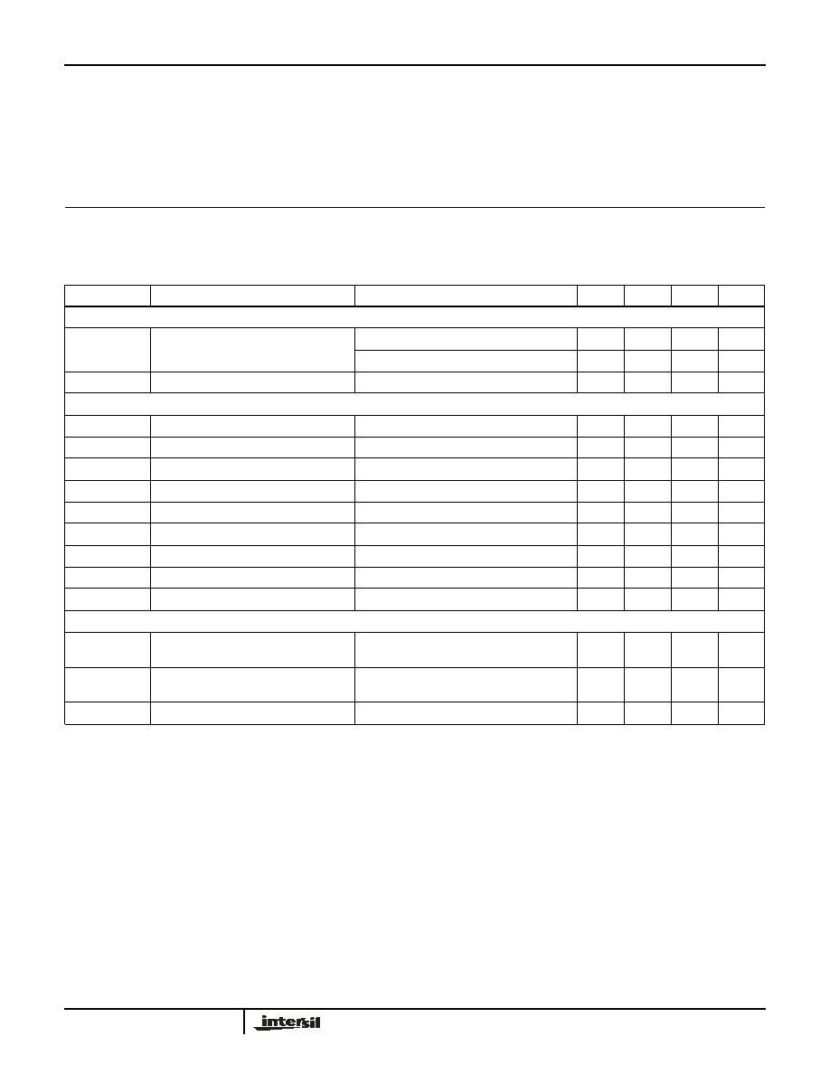
Absolute Maximum Ratings
(T
A
= 25°C)
Supply Voltage between V
S
and GND. . . . . . . . . . . . . . . . . . . .+18V
Supply Voltage between V
SD
and GND . . . . . . . V
S
and +7V (max)
Maximum Continuous Output Current . . . . . . . . . . . . . . . . . . . 30mA
Power Dissipation . . . . . . . . . . . . . . . . . . . . . . . . . . . . . See Curves
Maximum Die Temperature . . . . . . . . . . . . . . . . . . . . . . . . . . +125°C
Storage Temperature . . . . . . . . . . . . . . . . . . . . . . . .-65°C to +150°C
Ambient Operating Temperature . . . . . . . . . . . . . . . .-40°C to +85°C
CAUTION: Stresses above those listed in "Absolute Maximum Ratings" may cause permanent damage to the device. This is a stress only rating and operation of the
device at these or any other conditions above those indicated in the operational sections of this specification is not implied.
Electrical Specifications
V
S
= 15V, V
SD
= 5V, V
REFH
= 13V, V
REFL
= 2V, R
L
= 1.5k
and C
L
= 200pF to 0V, T
A
= 25°C, unless otherwise
specified.
PARAMETER
DESCRIPTION
CONDITIONS
MIN
TYP
MAX
UNIT
SUPPLY
I
S
Supply Current
EL5226
9
11
mA
EL5326
10
12
mA
I
SD
Digital Supply Current
0.9
3.2
mA
ANALOG
V
OL
Output Swing Low
Sinking 5mA (V
REFH
= 15V, V
REFL
= 0)
50
150
mV
V
OH
Output Swing High
Sourcing 5mA (V
REFH
= 15V, V
REFL
= 0)
14.85
14.95
V
I
SC
Short Circuit Current
R
L
= 10
150
240
mA
PSRR
Power Supply Rejection Ratio
V
S
+ is moved from 14V to 16V
45
65
dB
t
D
Program to Out Delay
4
ms
V
AC
Accuracy
20
mV
V
DROOP
Droop Voltage
1
2
mV/ms
R
INH
Input Resistance @ V
REFH
, V
REFL
34
k
REG
Load Regulation
I
OUT
= 5mA step
0.5
1.5
mV/mA
DIGITAL
V
IH
Logic 1 Input Voltage
V
SD
-
20%
V
V
IL
Logic 0 Input Voltage
20%*
V
SD
V
F
CLK
Clock Frequency
400
kHz
EL5226, EL5326
4
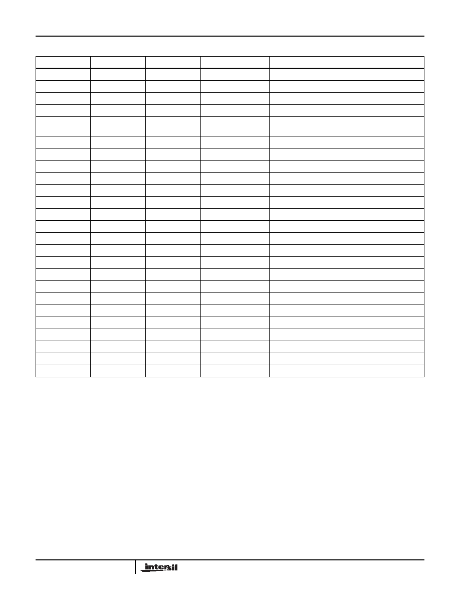
Pin Descriptions
EL5226
EL5326
PIN NAME
PIN TYPE
PIN FUNTION
1
1
STD_REG
Logic Input
Selects mode, high = standard, low = register mode
2
2
SCL
Logic Input
I
2
C clock
3
3
SDA
Logic Input
I
2
C data
4
4
OSC
Input/Output
Oscillator pin for synchronizing multiple chips
5
5
OSC_SELECT
Logic Input
Selects internal / external OSC source, high = external,
low = internal
6, 11
6, 11
VS
Analog Power
Power supply for analog circuit
7, 15, 28
7
NC
not connected
8
8
VSD
Digital Power
Power supply for digital circuit
9
9
REFH
Analog Reference Input High reference voltage
10
10
REFL
Analog Reference Input Low reference voltage
12, 19, 24
12, 18, 25
GND
Ground
Ground
13
13
CAP
Analog Bypass Pin
Decoupling capacitor for internal reference generator
14
14
DEV_ADDR0
Logic Input
I
2
C device address input, bit 0
16
17
OUTJ
Analog Output
Channel J programmable output
17
19
OUTI
Analog Output
Channel I programmable output
18
20
OUTH
Analog Output
Channel H programmable output
20
21
OUTG
Analog Output
Channel G programmable output
21
22
OUTF
Analog Output
Channel F programmable output
22
23
OUTE
Analog Output
Channel E programmable output
23
24
OUTD
Analog Output
Channel D programmable output
25
26
OUTC
Analog Output
Channel C programmable output
26
27
OUTB
Analog Output
Channel B programmable output
27
28
OUTA
Analog Output
Channel A programmable output
15
OUTL
Analog Output
Channel L programmable output
16
OUTK
Analog Output
Channel K programmable output
EL5226, EL5326
5
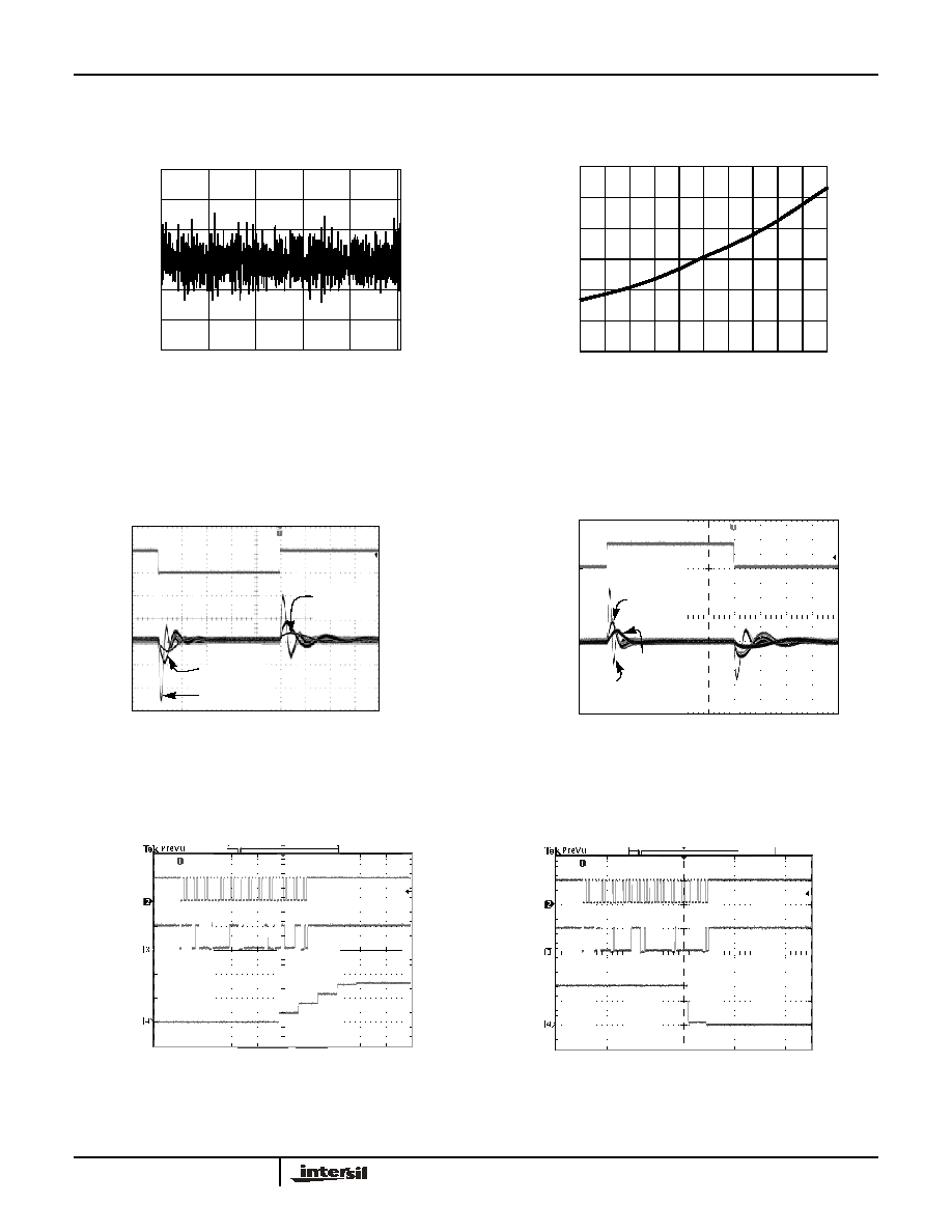
Typical Performance Curves
FIGURE 1. DIFFERENTIAL NONLINEARITY vs CODE
FIGURE 2. DIGITAL SUPPLY VOLTAGE vs DIGITAL SUPPLY
CURRENT
FIGURE 3. TRANSIENT LOAD REGULATION (SOURCING)
FIGURE 4. TRANSIENT LOAD REGULATION (SINKING)
FIGURE 5. LARGE SIGNAL RESPONSE (RISING FROM 0V
TO 8V)
FIGURE 6. LARGE SIGNAL RESPONSE (FALLING FROM 8V
TO 0V)
0.3
0.2
0.1
0
-0.1
-0.2
-0.3
10
210
410
610
810
1010
INPUT CODE
D
I
F
F
E
R
E
NT
I
A
L
NO
NL
I
N
E
A
RI
T
Y
(
L
SB
)
V
S
=15V, V
SD
=5V, V
REFH
=13V, V
REFL
=2V
1.2
1.0
0.6
0.2
0
4
4.8
5
I
SD
(mA)
0.8
0.4
V
S
=V
REFH
=15V
V
REFL
=0V
4.5
4.4
4.2
3
3.8
3.5
3.4
3.2
V
SD
(V)
0mA
5V
5mA/DIV
200mV/DIV
5mA
C
L
=180pF
C
L
=4.7nF
R
S
=20
C
L
=1nF
R
S
=20
V
S
=V
REFH
=15V
M=400ns/DIV
5mA
0mA
C
L
=1nF
R
S
=20
C
L
=180pF
V
S
=V
REFH
=15V
M=400ns/DIV
C
L
=4.7nF
R
S
=20
5V
SDA
0V
OUTPUT
SCLK
0V
5V
0V
10V
5V
M=400µs/DIV
SDA
OUTPUT
SCLK
M=400µs/DIV
EL5226, EL5326