Äîêóìåíòàöèÿ è îïèñàíèÿ www.docs.chipfind.ru
1
®
FN7506.0
EL5624A
6-Channel Buffer with High Power V
COM
The EL5624A integrates six gamma reference buffers with a
single high power V
COM
amplifier. Each gamma buffer has a
bandwidth of 12MHz and features a slew rate of 15V/µs. The
output current is rated at 30mA continuous, 140mA peak.
The V
COM
amplifier is rated for 260mA peak output current
and also features higher slew rate (70V/µs) and bandwidth
(35MHz) for use in error cancellation circuits.
The EL5624A is available in the 20-pin HTSSOP package
and is specified for operation over the -40°C to +85°C
temperature range.
Features
· 6 x gamma buffers
· Single high power V
COM
amplifier
· 260mA peak V
COM
output current
· Low power - just 8.5mA
· Pb-free available (RoHS compliant)
Applications
· TFT-LCD displays
· Flat panel monitors
· Notebook displays
· LCD-TVs
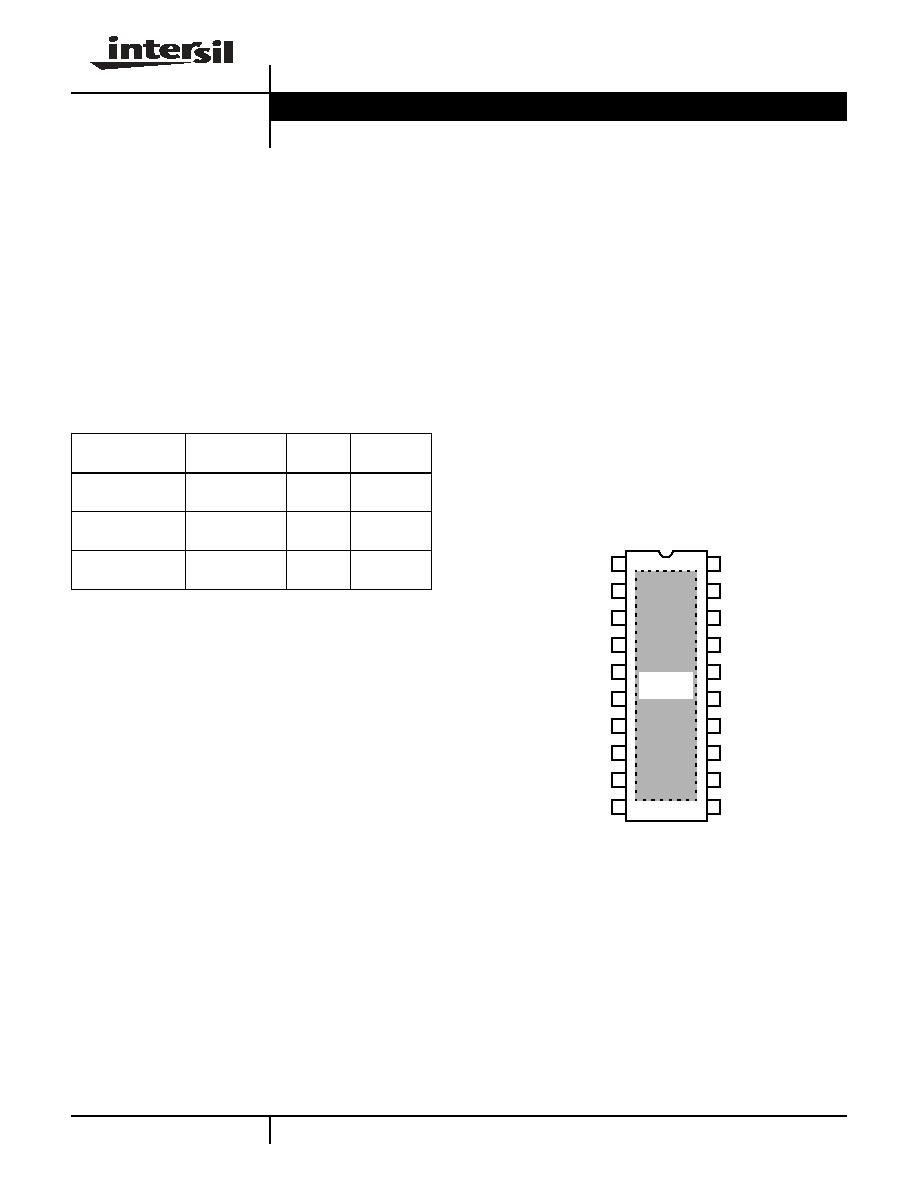
Pinout
EL5624A
(20-PIN HTSSOP)
TOP VIEW
Ordering Information
PART NUMBER
(See Note)
PACKAGE
(Pb-Free)
TAPE &
REEL
PKG. DWG. #
EL5624AIREZ
(See Note)
20-Pin HTSSOP
(Pb-free)
-
MDP0048
EL5624AIREZ-T7
(See Note)
20-Pin HTSSOP
(Pb-free)
7"
MDP0048
EL5624AIREZ-T13
(See Note)
20-Pin HTSSOP
(Pb-free)
13"
MDP0048
NOTE: Intersil Pb-free products employ special Pb-free material sets;
molding compounds/die attach materials and 100% matte tin plate
termination finish, which are RoHS compliant and compatible with
both SnPb and Pb-free soldering operations. Intersil Pb-free products
are MSL classified at Pb-free peak reflow temperatures that meet or
exceed the Pb-free requirements of IPC/JEDEC J STD-020.
1
2
3
4
16
15
14
13
5
6
7
12
11
9
8
10
20
19
18
17
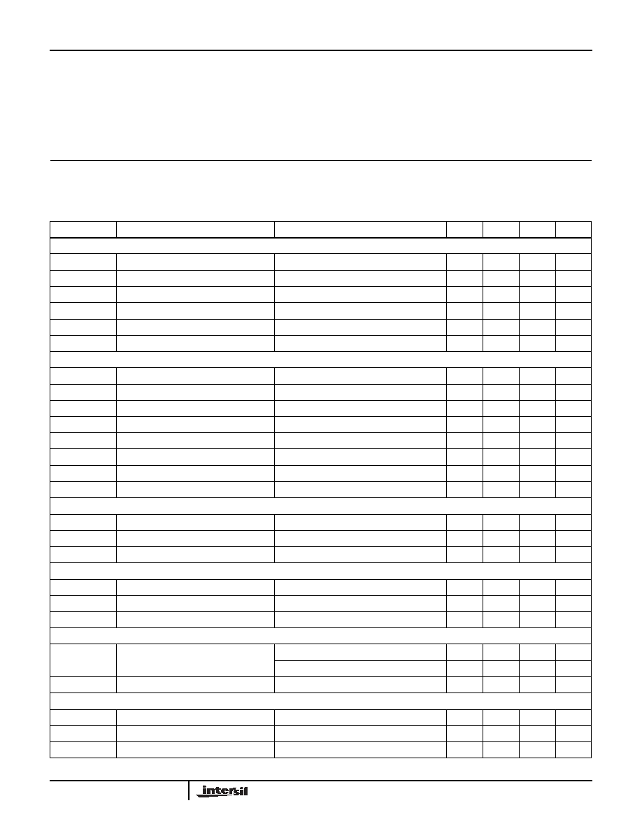
VIN1
VIN2
VIN3
VIN4
VS+
VS+
VIN5
VOUT1
VOUT2
VOUT3
VOUT4
VS-
VS-
VOUT5
VIN6
VINP
VINN
VOUT6
VOUT
NC
THERMAL
PAD*
* THERMAL PAD CONNECTED TO PIN 15 or 16 (V
S
-)
Data Sheet
February 14, 2005
CAUTION: These devices are sensitive to electrostatic discharge; follow proper IC Handling Procedures.
1-888-INTERSIL or 1-888-352-6832
|
Intersil (and design) is a registered trademark of Intersil Americas Inc.
Copyright Intersil Americas Inc. 2005. All Rights Reserved
All other trademarks mentioned are the property of their respective owners.
2
FN7506.0
February 14, 2005
NOTE: All parameters having Min/Max specifications are guaranteed. Typ values are for information purposes only. Unless otherwise noted, all tests
are at the specified temperature and are pulsed tests, therefore: T
J
= T
C
= T
A
Absolute Maximum Ratings
(T
A
= 25°C)
Supply Voltage between V
S
+ and V
S
- . . . . . . . . . . . . . . . . . . . .+18V
Input Voltage . . . . . . . . . . . . . . . . . . . . . . . . . . V
S
- -0.5V, V
S
+ +0.5V
Maximum Continuous Output Current (Buffer) . . . . . . . . . . . . 30mA
Maximum Continuous Output Current (V
COM
) . . . . . . . . . . . . 60mA
Power Dissipation . . . . . . . . . . . . . . . . . . . . . . . . . . . . . See Curves
Maximum Die Temperature . . . . . . . . . . . . . . . . . . . . . . . . . . +125°C
Storage Temperature . . . . . . . . . . . . . . . . . . . . . . . .-65°C to +150°C
Operating Conditions . . . . . . . . . . . . . . . . . . . . . . . . .-40°C to +85°C
CAUTION: Stresses above those listed in "Absolute Maximum Ratings" may cause permanent damage to the device. This is a stress only rating and operation of the
device at these or any other conditions above those indicated in the operational sections of this specification is not implied.
Electrical Specifications
V
S
+ = +15V, V
S
- = 0, R
L
= 10k
, C
L
= 10pF to 0V, Gain of V
COM
= 1, RLV
CM
= 1k
and T
A
= 25°C,
unless otherwise specified
PARAMETER
DESCRIPTION
CONDITIONS
MIN
TYP
MAX
UNIT
INPUT CHARACTERISTICS (REFERENCE BUFFERS)
V
OS
Input Offset Voltage
V
CM
= 0V
2
14
mV
TCV
OS
Average Offset Voltage Drift
(Note 1)
5
µV/
°C
I
B
Input Bias Current
V
CM
= 0V
2
50
nA
R
IN
Input Impedance
1
G
C
IN
Input Capacitance
1.35
pF
A
V
Voltage Gain
1V
V
OUT
14V
0.992
1.008
V/V
INPUT CHARACTERISTICS (V
COM
AMPLIFIER)
V
OS
Input Offset Voltage
V
CM
= 7.5V
1
15
mV
TCV
OS
Average Offset Voltage Drift
(Note 1)
5
µV/
°C
I
B
Input Bias Current
V
CM
= 7.5V
2
50
nA
R
IN
Input Impedance
1
G
C
IN
Input Capacitance
1.35
pF
V
REG
Load Regulation
V
COM
= 1.5V, -60mA < I
L
< 60mA
-20
+20
mV
A
VOL
Open Loop Gain
R
L
= 1k
55
75
dB
CMRR
Common Rejection Ratio
45
70
dB
OUTPUT CHARACTERISTICS (REFERENCE BUFFERS)
V
OL
Output Swing Low
I
L
= 7.5mA
50
150
mV
V
OH
Output Swing High
I
L
= 7.5mA
14.85
14.95
V
I
SC
Short Circuit Current
R
L
= 10
±200
±250
mA
OUTPUT CHARACTERISTICS (V
COM
AMPLIFIER)
V
OL
Output Swing Low
I
L
= -7.5mA
50
150
mV
V
OH
Output Swing High
I
L
= +7.5mA
14.85
14.95
V
I
SC
Short Circuit Current
R
L
= 10
±220
±260
mA
POWER SUPPLY PERFORMANCE
PSRR
Power Supply Rejection Ratio
Reference buffer V
S
from 4.5V to 15.5V
55
80
dB
V
COM
buffer, V
S
from 4.5V to 15.5V
55
80
dB
I
S
Total Supply Current
No load
8.5
10
mA
DYNAMIC PERFORMANCE (BUFFER AMPLIFIERS)
SR
Slew Rate (Note 2)
-4V
V
OUT
4V, 20% to 80%
50
70
V/µs
t
S
Settling to +0.1% (A
V
= +1)
(A
V
= +1), V
O
= 2V step
250
ns
BW
-3dB Bandwidth
R
L
= 10k
, C
L
= 10pF
12
MHz
EL5624A
3
FN7506.0
February 14, 2005
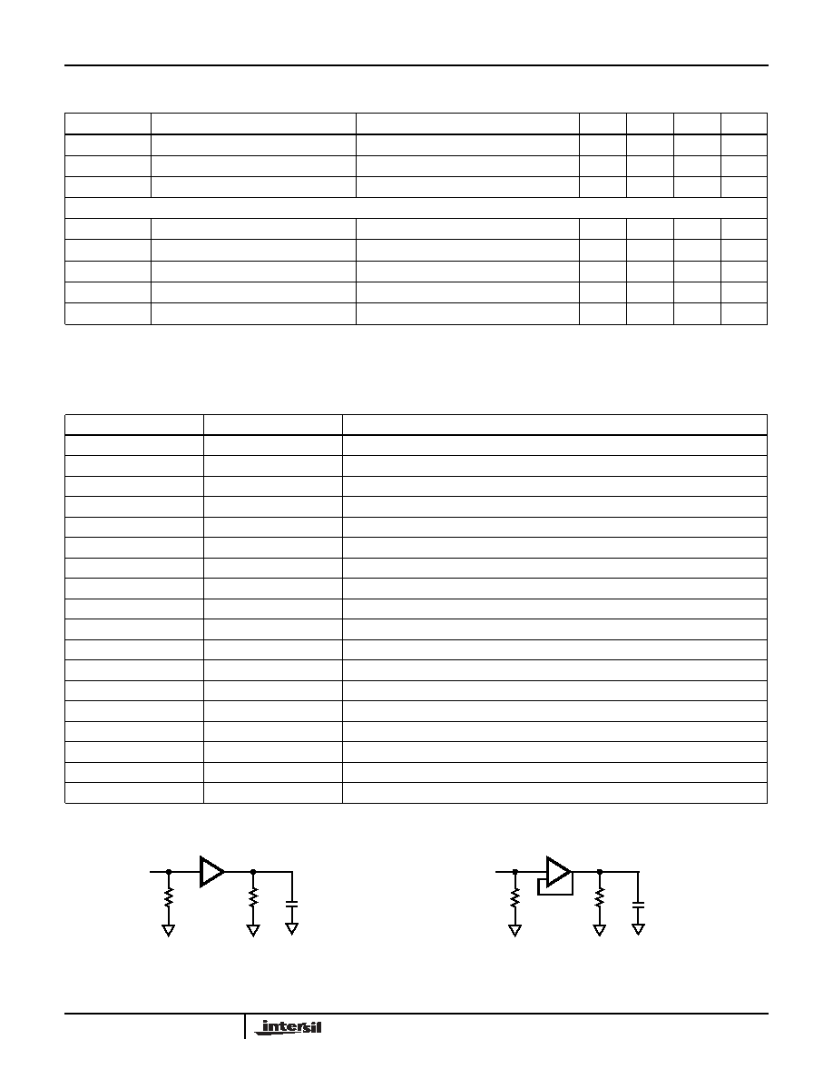
Test Circuits
GBWP
Gain-Bandwidth Product
R
L
= 10k
, C
L
= 10pF
8
MHz
PM
Phase Margin
R
L
= 10k
, C
L
= 10pF
50
°
CS
Channel Separation
f = 5MHz
75
dB
DYNAMIC PERFORMANCE (V
COM
AMPLIFIERS)
SR
Slew Rate (Note 2)
-4V
V
OUT
4V, 20% to 80%
60
70
V/µs
t
S
Settling to +0.1% (A
V
= +1)
(A
V
= +1), V
O
= 6V step
150
ns
BW
-3dB Bandwidth
R
L
= 1k
, C
L
= 2pF
35
MHz
GBWP
Gain-Bandwidth Product
R
L
= 1k
, C
L
= 2pF
20
MHz
PM
Phase Margin
R
L
= 1k
, C
L
= 2pF
50
°
NOTES:
1. Measured over operating temperature range
2. Slew rate is measured on rising and falling edges
Electrical Specifications
V
S
+ = +15V, V
S
- = 0, R
L
= 10k
, C
L
= 10pF to 0V, Gain of V
COM
= 1, RLV
CM
= 1k
and T
A
= 25°C,
unless otherwise specified
(Continued)
PARAMETER
DESCRIPTION
CONDITIONS
MIN
TYP
MAX
UNIT
Pin Descriptions
PIN NUMBER
PIN NAME
PIN FUNCTION
1
VIN1
Input
2
VIN2
Input
3
VIN3
Input
4
VIN4
Input
5, 6
VS+
Positive supply
9
VINP
Positive input - V
COM
10
VINN
Negative input - V
COM
11
NC
Not connected
12
VOUT
Output for V
COM
15, 16
VS-
Negative supply
17
VOUT4
Output
18
VOUT3
Output
19
VOUT2
Output
20
VOUT1
Output
7
VIN5
Input
8
VIN6
Input
14
VOUT5
Output
13
VOUT6
Output
50
10k
10pF
V
OUT
V
IN
50
1k
2pF
V
OUT
V
IN
FOR BUFFERS
FOR V
COM
+
-
EL5624A
4
FN7506.0
February 14, 2005
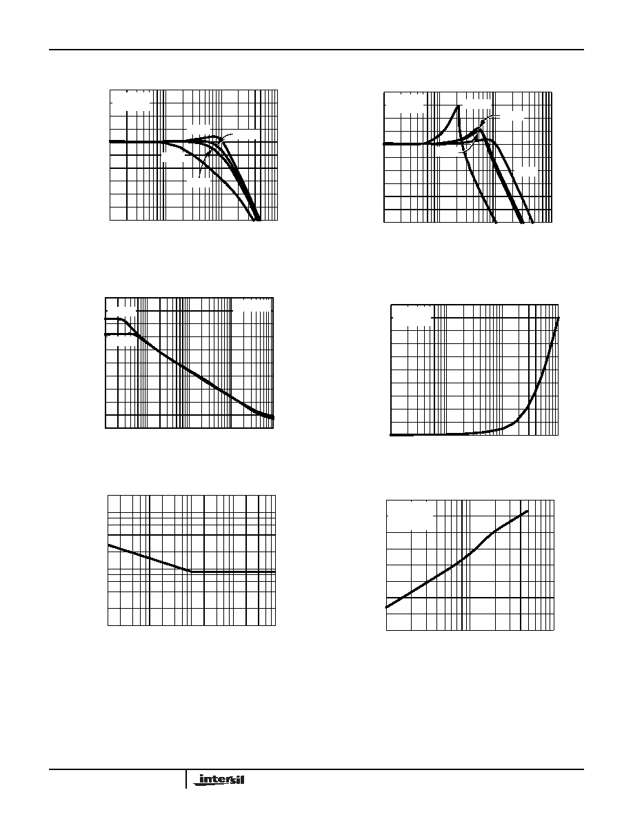
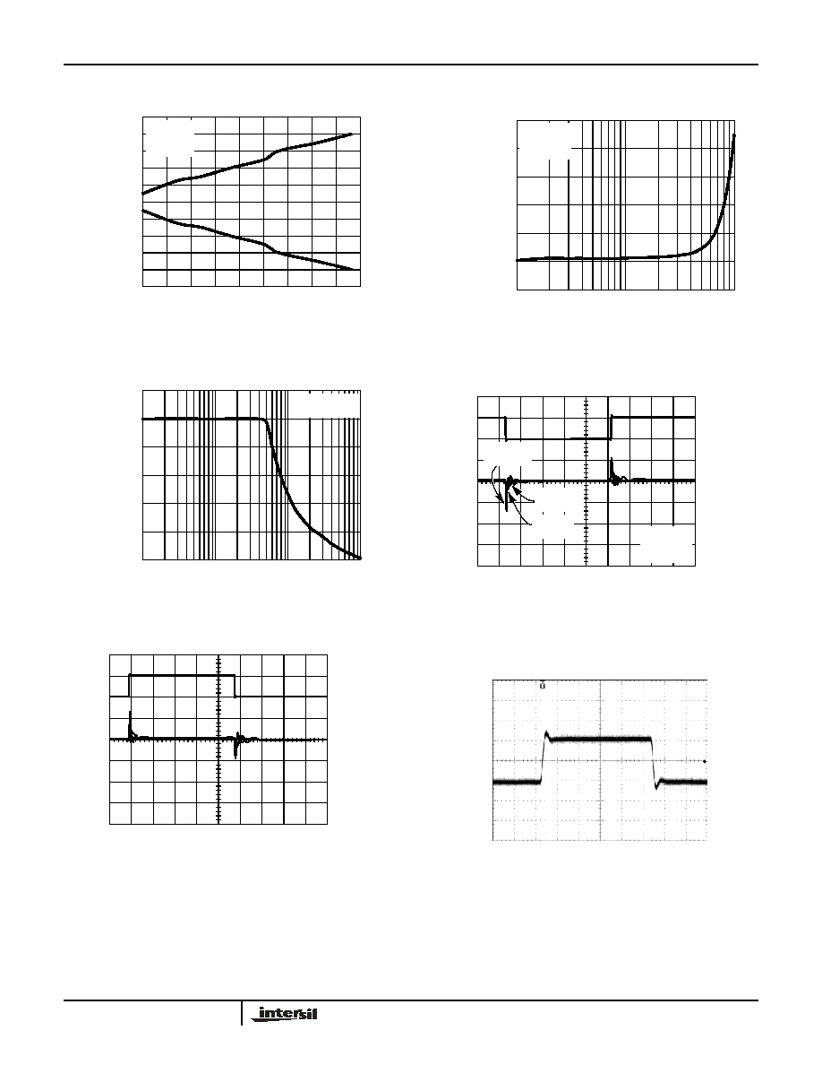
Typical Performance Curves
FIGURE 1. FREQUENCY RESPONSE FOR VARIOUS R
L
(BUFFER)
FIGURE 2. FREQUENCY RESPONSE FOR VARIOUS C
L
(BUFFER)
FIGURE 3. PSRR vs FREQUENCY (BUFFER)
FIGURE 4. OUTPUT IMPEDANCE vs FREQUENCY (BUFFER)
FIGURE 5. INPUT NOISE SPECIAL DENSITY vs FREQUENCY
(BUFFER)
FIGURE 6. OVERSHOOT vs LOAD CAPACITANCE (BUFFER)
N
O
RMAL
IZED MAGNITUDE (dB)
20
FREQUENCY (Hz)
V
S
=±7.5V
C
L
=10pF
10k
1k
150
562
10
-20
-30
0
-10
100K
1M
10M
100M
NORMALIZ
E
D
MAGNITUDE
(dB
)
20
FREQUENCY (Hz)
10
-20
-30
0
-10
100K
1M
10M
100M
V
S
=±7.5V
R
L
=10k
1000pF
12pF
100pF
47pF
PSRR+
PSRR-
V
S
=±7.5V
P
S
RR (
d
B)
100
FREQUENCY (Hz)
80
20
0
60
40
1K
10K
100K
10M
1M
V
S
=±7.5V
T
A
=25°C
OUT
P
UT
IMPEDANCE (
)
600
FREQUENCY (Hz)
480
120
0
360
240
100K
1M
10M
100M
VOL
T
AGE
NOIS
E (
n
V
/
Hz)
FREQUENCY (Hz)
100
10
1
10K
100K
1M
100M
10M
V
S
=±7.5V
R
L
=10k
V
IN
=100mV
O
VERS
H
O
O
T (%)
80
CAPACITANCE (pF)
60
10
0
40
20
10
100
1K
70
50
30
EL5624A
5
FN7506.0
February 14, 2005
FIGURE 7. SETTLING TIME vs STEP SIZE (BUFFER)
FIGURE 8. TOTAL HARMONIC DISTORTION + NOISE vs
FREQUENCY (BUFFER)
FIGURE 9. OUTPUT SWING vs FREQUENCY (BUFFER)
FIGURE 10. TRANSIENT LOAD REGULATION - SOURCING
(BUFFER)
FIGURE 11. TRANSIENT LOAD REGULATION -SINKING
(BUFFER)
FIGURE 12. SMALL SIGNAL TRANSIENT RESPONSE
(BUFFER)
Typical Performance Curves
(Continued)
V
S
=±7.5V
R
L
=10k
C
L
=12pF
STEP SI
ZE (V)
10
SETTLING TIME (ns)
2
-10
-6
200
400
650
6
-2
250
450
300
500
350
550 600
V
S
=±5V
R
L
=10k
V
IN
=2V
P-P
T
HD +
NOIS
E (%
)
0.018
FREQUENCY (Hz)
0.014
0.006
0.01
1K
10K
100K
0.016
0.012
0.008
V
S
=±5V
R
L
=10k
V
OP-P
(V
)
12
FREQUENCY (Hz)
10
2
0
6
4
10K
100K
1M
10M
8
0mA
5mA
0V
5mA/DIV
500mA/DIV
M=1µs/DIV
V
S
=±7.5V
V
IN
=0V
R
S
=0
C
L
=200pF
R
S
=10
C
L
=4.7pF
R
S
=10
C
L
=1nF
200ns/DIV
50mV/DIV
V
S
=±7.5V
R
L
=10k
C
L
=12pF
EL5624A