 | –≠–ª–µ–∫—Ç—Ä–æ–Ω–Ω—ã–π –∫–æ–º–ø–æ–Ω–µ–Ω—Ç: EL6202 | –°–∫–∞—á–∞—Ç—å:  PDF PDF  ZIP ZIP |

1
Æ
FN7217.1
CAUTION: These devices are sensitive to electrostatic discharge; follow proper IC Handling Procedures.
1-888-INTERSIL or 321-724-7143
|
Intersil (and design) is a registered trademark of Intersil Americas Inc.
Copyright © Intersil Americas Inc. 2003-2004. All Rights Reserved. Elantec is a registered trademark of Elantec Semiconductor, Inc.
All other trademarks mentioned are the property of their respective owners.
EL6202
Laser Driver Oscillator
The EL6202 consists of a variable
amplitude, push only, oscillator that
also supplies the laser DC current. It is
designed to easily interface to existing ROM controllers,
reducing parts count, and power dissipation.
The reduction of parts count and the small package allows
the oscillator to be placed closer to the laser, thus reducing
EMI. Also, the turn-on and turn-off edges are slew rate
limited to reduce higher harmonics.
The total current drawn from the power supply can be less
than the laser threshold current due to the unique push-only
modulation method. The average current is less than the
peak oscillator current, and can be less than half of the
oscillator current. The power control current supplied from
the main board is reduced to less than 2mA.
One external resistor sets the oscillator frequency. A current
applied to the I
IN
terminal determines the amplitude of the
oscillator and laser DC current. If the oscillator amplitude is
set very low, the output and oscillator are disabled. The part
is available in the space-saving SOT23-5 package. It is
specified for operation from 0∞C to +70∞C.
Pinout
EL6202
(5-PIN SOT-23)
TOP VIEW
Features
∑ Low power dissipation
∑ Reduced parts count from the conventional solution
∑ User-selectable frequency from 60MHz to 600MHz
controlled with a single resistor
∑ User-selectable amplitude from 15mA
PK-PK
to
100mA
PK-PK
controlled by 0.3mA to 2mA input current
∑ Auto turn-off threshold
∑ Soft edges for reduced EMI
∑ Small SOT23-5 package
Applications
∑ DVD players
∑ DVD-ROM drives
∑ Combo drives
∑ MO drives
∑ General purpose laser noise reduction
∑ Local oscillator capability
1
2
3
5
4
VDD
RFREQ
GND
IOUT
IIN
Ordering Information
PART NUMBER
PACKAGE
TAPE & REEL PKG. DWG. #
EL6202CW-T7
5-Pin SOT-23
7" (3K pcs)
MDP0038
EL6202CW-T7A
5-Pin SOT-23
7" (250 pcs)
MDP0038
Data Sheet
June 11, 2004

2
Absolute Maximum Ratings
(T
A
= 25∞C)
Voltages Applied to:
V
DD
. . . . . . . . . . . . . . . . . . . . . . . . . . . . . . . . . -0.5V to +6.0V
I
OUT
. . . . . . . . . . . . . . . . . . . . . . . . . . . . . . . . -0.5V to +6.0V
R
FREQ
, I
IN
. . . . . . . . . . . . . . . . . . . . . . . . . . . -0.5V to +6.0V
Operating Ambient Temperature . . . . . . . . . . . . . . . . . 0∞C to +70∞C
Maximum Die Operating Temperature . . . . . . . . . . . . . . . . . . +150∞C
Storage Temperature Range . . . . . . . . . . . . . . . . . . -65∞C to +150∞C
Output Current . . . . . . . . . . . . . . . . . . . . . . . . . . . . . . . 100mA
PK-PK
Power Dissipation (max) . . . . . . . . . . . . . . . . . . . . . . . . See Curves
CAUTION: Stresses above those listed in "Absolute Maximum Ratings" may cause permanent damage to the device. This is a stress only rating and operation of the
device at these or any other conditions above those indicated in the operational sections of this specification is not implied.
IMPORTANT NOTE: All parameters having Min/Max specifications are guaranteed. Typical values are for information purposes only. Unless otherwise noted, all tests
are at the specified temperature and are pulsed tests, therefore: T
J
= T
C
= T
A
Supply & Reference Voltage Characteristics
V
DD
= +5V, T
A
= 25∞C, R
L
= 10
, R
FREQ
= 5210
(F
OSC
= 350MHz), I
IN
= 1mA
(I
OUT
= 50mA
P-P
measured at 60MHz), V
OUT
= 2.2V
PARAMETER
DESCRIPTION
CONDITIONS
MIN
TYP
MAX
UNIT
PSOR
Power Supply Operating Range
4.5
5.5
V
I
SO
Supply Current Disabled
I
IN
100µA
550
750
µA
I
STYP
Supply Current Typical Conditions
R
FREQ
= 5.21k
(includes laser current)
25
30
35
mA
I
SLO
Supply Current Low Conditions
R
FREQ
= 30.5k
, I
IN
= 300µA (includes laser
current)
10
mA
I
SHI
Supply Current High Conditions
R
FREQ
= 3.05k
,
I
IN
= 2mA (includes laser current)
53
mA
V
FREQ
Voltage at R
FREQ
Pin
1.27
V
R
IN
Input Impedance
500
Oscillator Characteristics
V
DD
= +5V, T
A
= 25∞C, R
L
= 10
, R
FREQ
= 5210
(F
OSC
= 350MHz), I
IN
= 1mA (I
OUT
= 50mA
P-P
measured
at 60MHz), V
OUT
= 2.2V
PARAMETER
DESCRIPTION
CONDITIONS
MIN
TYP
MAX
UNIT
F
OSC
Frequency Tolerance
Unit-unit frequency variation
300
350
400
MHz
F
HIGH
Frequency Range High
R
FREQ
= 3.05k
600
MHz
F
LOW
Frequency Range Low
R
FREQ
= 30.5k
60
MHz
TC
OSC
Frequency Temperature Sensitivity
0∞C to 70∞C ambient
50
ppm/∞C
PSRR
OSC
Frequency Change
F/F
V
DD
from 4.5V to 5.5V
1
%
Driver Characteristics
V
DD
= +5V, T
A
= 25∞C, R
L
= 10
, R
FREQ
= 30.5k
(F
OSC
= 60MHz), I
IN
= 1mA (I
OUT
= 50mA
P-P
measured at
60MHz), V
OUT
= 2.2V
PARAMETER
DESCRIPTION
CONDITIONS
MIN
TYP
MAX
UNIT
AMP
HIGH
Amplitude Range High
I
IN
= 2mA
100
mA
P-P
AMP
LOW
Amplitude Range Low
I
IN
= 300µA
15
mA
P-P
I
AVG
Average Output Current @ 2.2V
R
FREQ
= 5210
19
mA
I
OUTP-P
Output Current Tolerance
Defined as one standard deviation
2
%
Duty Cycle
Output Push Time/Cycle Time
R
FREQ
= 5210
43
%
PSRR
AMP
Amplitude Change of Output
I/I
VDD from 4.5V to 5.5V
-54
dB
T
ON
Auto Turn-on Time
Input current step from 0mA to 1mA
15
µs
T
OFF
Auto Turn-off Time
Input current step from 1mA to 0mA
0.5
µs
IN
OUT
I
OUT
Current Output Noise Density
R
FREQ
= 5490
,
F
MEASURE
= 10MHz
2.5
nA/
Hz
EL6202

3
Control Table
I
IN
I
OUT
100µA
OFF
300µA
Normal Operation
Pin Descriptions
PIN NUMBER
PIN NAME
PIN DESCRIPTION
1
VDD
Positive power for chip and laser driver (3.3V - 5V)
2
GND
Chip ground pin (0V)
3
IOUT
Current output to laser anode
4
IIN
Set pin for output current amplitude
5
RFREQ
Set pin for oscillator frequency
Recommended Operating Conditions
V
DD
. . . . . . . . . . . . . . . . . . . . . . . . . . . . . . . . . . . . . . . . . . 5V ±10%
V
OUT
. . . . . . . . . . . . . . . . . . . . . . . . . . . . . . . . . . . . . . . . . . . . 2V-3V
R
FREQ
. . . . . . . . . . . . . . . . . . . . . . . . . . . . . . . . . . . . . . . . 3k
(min)
I
IN
. . . . . . . . . . . . . . . . . . . . . . . . . . . . . . . . . . . . . . . . . . . 2mA (max)
F
OSC
. . . . . . . . . . . . . . . . . . . . . . . . . . . . . . . . . . . . . . . .60-600MHz
I
OUT
. . . . . . . . . . . . . . . . . . . . . . . . . . . . . . . . . . . . . 15-100mA
PK-PK
EL6202

4
Typical Performance Curves
V
DD
= 5V, T
A
= 25∞C, R
L
= 10
, R
FREQ
= 5.21k
, I
IN
= 1mA, V
OUT
= 2.2V unless otherwise specified.
FIGURE 1. FREQUENCY DISTRIBUTION
FIGURE 2. FREQUENCY DRIFT WITH TEMPERATURE
FIGURE 3. FREQUENCY vs R
FREQ
FIGURE 4. FREQUENCY vs 1/R
FREQ
FIGURE 5. AMPLITUDE vs I
IN
FIGURE 6. FREQUENCY vs SUPPLY VOLTAGE
NU
MBER O
F
P
A
R
T
S
0
100
500
FREQUENCY (MHz)
310
318
334
350
366
326
342
358
200
300
400
374
382
390
Typical
Production
Distortion
NU
MBER O
F
P
A
R
T
S
0
1
8
FREQUENCY TC (ppm/∞C)
6
30
54
18
42
3
5
7
66
78
90
Measured from
-40∞C to +85∞C
2
4
6
FREQ
U
E
NC
Y (M
Hz)
0
200
400
500
600
700
R
FREQ
(k
)
0
5
15
25
35
10
20
30
100
300
Frequency=1824 * 1k
/ R
FREQ
(MHz)
FREQ
U
E
NC
Y (M
Hz)
0
200
400
500
600
700
1k
/ R
FREQ
0
0.05
0.15
0.25
0.35
0.1
0.2
0.3
100
300
Frequency=1824 * 1k
/ R
FREQ
(MHz)
AM
PLITUD
E (mA
PK-PK
)
0
20
40
60
80
100
I
IN
(mA)
0
1
2
Amplitude = 50 * I
IN
FREQ
UEN
C
Y (
M
Hz)
340
345
355
360
SUPPLY VOLTAGE (V)
4.4
4.6
4.8
5.2
5.6
5
5.4
350
EL6202

5
Block Diagram
FIGURE 7. FREQUENCY vs TEMPERATURE
Typical Performance Curves
V
DD
= 5V, T
A
= 25∞C, R
L
= 10
, R
FREQ
= 5.21k
, I
IN
= 1mA, V
OUT
= 2.2V unless otherwise specified.
FREQ
UEN
C
Y (M
Hz)
300
320
380
400
AMBIENT TEMPERATURE (∞C)
-50
0
150
50
100
340
360
1
3
6
4
BANDGAP
REFERENCE
DRIVER
AUTO
SHUT-OFF
OSCILLATOR
V
DD
I
OUT
R
FREQ
IN
2
GND
EL6202

6
Typical Application Circuit
Applications Information
Product Description
The EL6202 is a solid state, low-power, high-speed laser
modulation oscillator with external resistor-adjustable
operating frequency. It is designed to interface easily to laser
diodes to break up optical feedback resonant modes and
thereby reduce laser noise. The output of the EL6202 is
composed of a push current source switched at the oscillator
frequency. The output and oscillator are automatically
disabled for power saving when the average input current
drops to less than 100µA. The EL6202 has the operating
frequency from 60MHz to 600MHz and the output current
from 10mA
P-P
to 100mA
P-P
. The supply current is only
30mA (includes laser current) for the output current of
50mA
P-P
at the operating frequency of 350MHz.
1
2
3
5
4
VDD1
RFREQ
GND
IOUT
IIN
CONTROLLER
LOOP
COMPENSATION-
NOISE
REDUCTION
CAPACITOR
FREQUENCY
SETTING
RESISTOR
EMI
REDUCTION
SUPPLY
FILTER
GAIN
SETTING
RESISTOR
TYPICAL
ROM LASER
DRIVER
LASER DIODE
PHOTO DIODE
BEAD
+5V
FLEX
GND
0.1µF
4.7µF
EMI
BLOCKING
RESISTOR
Either the high current controller resistor can be
reduced to 2mA full scale, or the transistor and resistor
can be replaced with a resistor from the controller DAC.
DAC
LASER OUTPUT
POWER
LASER CURRENT
0mW
~10mW
0mA
~60mA
OSCILLATOR CURRENT
LASER OUTPUT POWER
THRESHOLD
CURRENT
optional
EL6202

7
Theory of Operation
A typical semiconductor laser will emit a small amount of
incoherent light at low values of forward laser current. But
after the threshold current is reached, the laser will emit
coherent light. Further increases in the forward current will
cause rapid increases in laser output power. A typical
threshold current is 35mA and a typical slope efficiency is
0.7mW/mA.
When the laser is lasing, it will often change its mode of
operation slightly, due to changes in current, temperature, or
optical feedback into the laser. In a DVD-ROM, the optical
feedback from the moving disk forms a significant noise
factor due to feedback-induced mode hopping. In addition to
the mode hopping noise, a diode laser will roughly have a
constant noise level regardless of the power level when a
threshold current is exceeded.
The oscillator is designed to produce a low noise oscillating
current that is provided to the laser diode. The current is to
cause the laser power to change at the oscillator frequency.
This change causes the laser to go through rapid mode
hopping. The low frequency component of laser power noise
due to mode hopping is translated up to sidebands around
the oscillator frequency by this action. Since the oscillator
frequency can be filtered out of the low frequency read and
serve channels, the net result is that the laser noise seems
to be reduced. The second source of laser noise reduction is
caused by the increase in the laser power above the average
laser power during the pushing-current time. The signal-to-
noise ratio (SNR) of the output power is better at higher laser
powers because of the almost constant noise power when a
threshold current is exceeded. In addition, when the laser is
off during no output current time, the noise is also very low.
Setting the I
IN
Current
By looking the typical application circuit, it can be seen that
the push only oscillator is more efficient at the laser than the
conventional push-pull oscillator. The significant current from
the main board is reduced to be I
IN
(
2mA), while the
oscillator takes on the role of supplying the total laser
current.
The I
IN
current is the previous read current (reduced in
amplitude). Thus it does not need to be set, since it is within
the control loop. The current capability of the external source
for I
IN
should be made large enough to power the worst,
hottest old laser.
R
FREQ
Pin Interfacing
Figure 8 shows an equivalent circuit of pins associated with
the R
FREQ
resistor. V
REF
is roughly 1.27V. The resistor
R
FREQ
should be connected to the non-load side of the
power ground to avoid noise. This resistor should also return
to the EL6202's ground very directly to prevent noise pickup.
They also should have minimal capacitance to ground.
Trimmer resistors can be used to adjust initial operating
points.
External voltage sources can be coupled to the R
FREQ
pin
to effect frequency modulation or adjustment. It is
recommended that a coupling resistor be installed in series
with the control voltage and mounted directly next to the pin.
This will keep the inevitable high-frequency noise of the
EL6202's local environment from propagating to the
modulation source, and it will keep parasitic capacitance at
the pin minimized.
Supply Bypassing and Grounding
The resistance of bypass-capacitors and the inductance of
bonding wires prevent perfect bypass action, and 150mV
P-P
noise on the power lines is common. There needs to be a
lossy series bead inductance and secondary bypass on the
supply side to control signals from propagating down the
wires. Figure 9 shows the typical connection.
Also important is circuit-board layout. At the EL6202's
operating frequencies, even the ground plane is not low-
impedance. High frequency current will create voltage drops
in the ground plane. Figure 10 shows the output current loop.
-
+
PIN
V
REF
FIGURE 8. R
FREQ
PIN INTERFACE
FIGURE 9. RECOMMENDED SUPPLY BYPASSING
+5V
V
S
L Series: 70
reactance at
300MHz (see text)
0.1µF
Chip
EL6202
GND
0.1µF
Chip
FIGURE 10. OUTPUT CURRENT LOOP
SOURCING CURRENT LOOP
SUPPLY
BYPASS
LOAD
R
FREQ
R
AMP
GND
(8-PIN
PACKAGE)
EL6202
8
All Intersil U.S. products are manufactured, assembled and tested utilizing ISO9000 quality systems.
Intersil Corporation's quality certifications can be viewed at www.intersil.com/design/quality
Intersil products are sold by description only. Intersil Corporation reserves the right to make changes in circuit design, software and/or specifications at any time without
notice. Accordingly, the reader is cautioned to verify that data sheets are current before placing orders. Information furnished by Intersil is believed to be accurate and
reliable. However, no responsibility is assumed by Intersil or its subsidiaries for its use; nor for any infringements of patents or other rights of third parties which may result
from its use. No license is granted by implication or otherwise under any patent or patent rights of Intersil or its subsidiaries.
For information regarding Intersil Corporation and its products, see www.intersil.com
For the current loop, the current flows through the supply
bypass-capacitor. The ground end of the bypass thus should
be connected directly to the EL6202 ground pin and laser
ground. A long ground return path will cause the bypass
capacitor currents to generate voltage drops in the ground
plane of the circuit board, and other components (such as
R
FREQ
) will pick this up as an interfering signal. Similarly,
the ground return of the load should be considered, as noisy
and other grounded components should not connect to this
path. Slotting the ground plane around the load's return will
reduce adjacent grounded components from seeing the
noise.
Power Dissipation
It is important to calculate the maximum junction
temperature for the application to determine if the conditions
need to be modified for the oscillator to remain in the safe
operating area.
The maximum power dissipation allowed in a package is
determined according to:
where:
P
DMAX
= Maximum power dissipation in the package
T
JMAX
= Maximum junction temperature
T
AMAX
= Maximum ambient temperature
JA
= Thermal resistance of the package
The supply current of the EL6202 depends on the peak-to-
peak output current and the operating frequency which is
determined by resistor R
FREQ
. The supply current can be
predicted approximately by the following equations:
The power dissipation can be calculated from the following
equation:
Here, V
SUP
is the supply voltage and V
LAS
is the average
voltage of the laser diode. Figure 11 provides a convenient
way to see if the device may overheat. The maximum safe
power dissipation can be found graphically, based on the
ambient temperature and JEDEC standard single layer PCB.
For flex circuits, the
JA
could be higher. By using the
previous equation, it is possible to estimate if P
D
exceeds
the device's power derating curve. To ensure proper
operation, it is important to observe the recommended
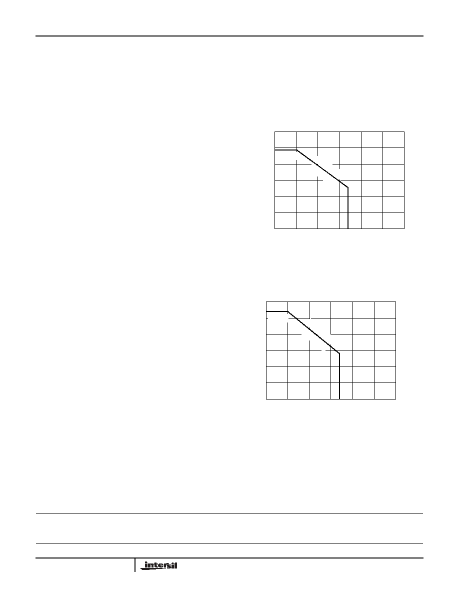
derating curve shown in Figure 12.
P
DMAX
T
JMAX
- T
AMAX
JA
---------------------------------------------
=
I
SUP1
35mA
1k
◊
R
FREQ
----------------------------------
0.5mA
+
=
I
SUP2
50
I
IN
0.5
◊
◊
=
P
D
V
SUP
I
SUP1
V
(
SUP
- V
LAS
)
I
SUP2
◊
+
◊
=
FIGURE 11. PACKAGE POWER DISSIPATION vs
AMBIENT TEMPERATURE
0.6
0.5
0.4
0.3
0.2
0.1
0
0
25
50
75
100
125
150
AMBIENT TEMPERATURE (∞C)
PO
WER DISSIP
A
T
I
O
N (W
)
85
JEDEC JESD51-3 LOW EFFECTIVE THERMAL
CONDUCTIVITY TEST BOARD
488mW
5-P
in S
OT
-23
JA =
25
6∞C
/W
FIGURE 12. PACKAGE POWER DISSIPATION vs
AMBIENT TEMPERATURE
0.6
0.5
0.4
0.3
0.2
0.1
0
0
25
50
75
100
125
150
AMBIENT TEMPERATURE (∞C)
P
O
WE
R DISS
IP
A
T
ION (W
)
85
543mW
5-P
in
S
O
T-2
3
JA =
23
0∞C
/W
JEDEC JESD51-7 HIGH EFFECTIVE THERMAL
CONDUCTIVITY TEST BOARD
EL6202