1
Æ
FN7278.1
EL7154
High Speed, Monolithic Pin Driver
The EL7154 3-state pin driver is particularly well suited for
ATE and level shifting applications. The 4A peak drive
capability, makes the EL7154 an excellent choice when
driving high speed capacitive lines.
The p-channel MOSFET is completely isolated from the
power supply, providing a high degree of flexibility. Pin (7)
can be grounded, and the output can be taken from pin (8)
when a "source follower" output is desired. Then n-channel
MOSFET has an isolated drain, but shares a common bus
with pre-drivers and level shifter circuits. This is necessary to
ensure that the nchannel device can turn off effectively when
V
L
goes below GND. In some power-FET and IGBT
applications, negative drive is desirable to insure effective
turn-off. The EL7154 can be used in these applications by
returning V
L
to a moderate negative potential.
Pinout
Manufactured under U.S. Patent Nos. 5,334,883, #5,341,047,
#5,352,578, #5,352,389, #5,351,012, #5,374,898
Features
∑ Comparatively low cost
∑ 3-State output
∑ 3V and 5V Input compatible
∑ Clocking speeds up to 10MHz
∑ 20ns Switching/delay time
∑ 4A Peak drive
∑ Isolated drains
∑ Low output impedance--2.5
∑ Low quiescent current--5mA
∑ Wide operating voltage--4.5V≠16V
∑ Isolated P-channel device
∑ Separate ground and V
L
pins
∑
Pb-Free available (RoHS compliant)
Applications
∑ Loaded circuit board testers
∑ Digital testers
∑ Level shifting below GND
∑ IGBT drivers
∑ CCD drivers
Truth Table
3-STATE
INPUT
P
OUT
N
OUT
0
0
Open
Open
0
1
Open
Open
1
0
HIGH
Open
1
1
Open
LOW
EL7154
(8-PIN PDIP, SOIC)
TOP VIEW
Ordering Information
PART NUMBER
PACKAGE
TAPE &
REEL
PKG. DWG. #
EL7154CN
8-Pin PDIP
-
MDP0031
EL7154CS
8-Pin SOIC
-
MDP0027
EL7154CS-T7
8-Pin SOIC
7"
MDP0027
EL7154CS-T13
8-Pin SOIC
13"
MDP0027
EL7154CSZ
(See Note)
8-Pin SOIC
(Pb-free)
-
MDP0027
EL7154CSZ-T7
(See Note)
8-Pin SOIC
(Pb-free)
7"
MDP0027
EL7154CSZ-T13
(See Note)
8-Pin SOIC
(Pb-free)
13"
MDP0027
NOTE: Intersil Pb-free products employ special Pb-free material sets;
molding compounds/die attach materials and 100% matte tin plate
termination finish, which are RoHS compliant and compatible with
both SnPb and Pb-free soldering operations. Intersil Pb-free products
are MSL classified at Pb-free peak reflow temperatures that meet or
exceed the Pb-free requirements of IPC/JEDEC J STD-020.
Data Sheet
May 6, 2005
CAUTION: These devices are sensitive to electrostatic discharge; follow proper IC Handling Procedures.
1-888-INTERSIL or 1-888-352-6832
|
Intersil (and design) is a registered trademark of Intersil Americas Inc.
Copyright Intersil Americas Inc. 1996, 2003, 2005. All Rights Reserved
All other trademarks mentioned are the property of their respective owners.

3
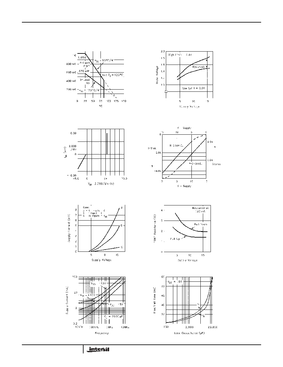
Absolute Maximum Ratings
(T
A
= 25∞C)
Supply (V
DD
to V
L
; V
H
≠V
L
, V
H
to GND),
V+ to V
H
. . . . . . . . . . . . . . . . . . . . . . . . . . . . . . . . . . . . . . . . . . 16.5V
V
L
to GND . . . . . . . . . . . . . . . . . . . . . . . . . . . . . . . . . . . . . . . . . . -5V
Input Pins . . . . . . . . . . . . . . . . . -0.3V below V
L
to +0.3V above V
DD
Peak Output Current . . . . . . . . . . . . . . . . . . . . . . . . . . . . . . . . . . .4A
Storage Temperature Range . . . . . . . . . . . . . . . . . .-65∞C to +150∞C
Ambient Operating Temperature . . . . . . . . . . . . . . . .-40∞C to +85∞C
Operating Junction Temperature . . . . . . . . . . . . . . . . . . . . . . . 125∞C
Power Dissipation
SOIC . . . . . . . . . . . . . . . . . . . . . . . . . . . . . . . . . . . . . .570mW
PDIP . . . . . . . . . . . . . . . . . . . . . . . . . . . . . . . . . . . . .1050mW
CAUTION: Stresses above those listed in "Absolute Maximum Ratings" may cause permanent damage to the device. This is a stress only rating and operation of the
device at these or any other conditions above those indicated in the operational sections of this specification is not implied.
IMPORTANT NOTE: All parameters having Min/Max specifications are guaranteed. Typical values are for information purposes only. Unless otherwise noted, all tests
are at the specified temperature and are pulsed tests, therefore: T
J
= T
C
= T
A
DC Electrical Specifications
T
A
= 25∞C, V
DD
= +12V, V
H
= +12V, V
L
= -3V, unless otherwise specified
PARAMETER
DESCRIPTION
TEST CONDITIONS
MIN
TYP
MAX
UNITS
INPUT
V
IH
Logic "1" Input Voltage
2.4
V
I
IH
Logic "1" Input Current
V
IH
= V
DD
0.1
10
µA
V
IL
Logic "0" Input Voltage
0.6
V
I
IL
Logic "0" Input Current
V
IL
= 0V
0.1
10
µA
V
HVS
Input Hysteresis
0.3
V
OUTPUT
R
OH
Pull-Up Resistance
I
OUT
= -100mA
1.5
4
R
OL
Pull-Down Resistance
I
OUT
= +100mA
2
4
I
OUT
Output Leakage Current
V
DD
/GND
0.2
10
µA
I
PK
Peak Output Current
Source
Sink
4.0
4.0
A
I
DC
Continuous Output Current
Source/Sink
200
mA
POWER SUPPLY
I
S
Power Supply Current
Inputs = V
DD
1
2.5
mA
V
S
Operating Voltage
4.5
16
V
I
G
Current to GND (Pin 4)
1
10
µA
I
H
Off Leakage at V
H
Pin 8 = 0V
1
10
µA
AC Electrical Specifications
T
A
= 25∞C unless otherwise specified
PARAMETER
DESCRIPTION
TEST CONDITIONS
MIN
TYP
MAX
UNITS
SWITCHING CHARACTERISTICS (V
DD
= V
H
= 12V; V
L
= -3V)
t
R
Rise Time
C
L
= 100pF
4
25
ns
C
L
= 2000pF
20
t
F
Fall Time
C
L
= 100pF
4
25
ns
C
L
= 2000pF
20
t
D-1
Turn-Off Delay Time
C
L
= 2000pF
20
25
ns
t
D-2
Turn-On Delay Time
C
L
= 2000pF
10
25
ns
t
D-1
3-State Delay
25
ns
t
D-2
3-State Delay
25
ns
EL7154