1
®
FN7284
CAUTION: These devices are sensitive to electrostatic discharge; follow proper IC Handling Procedures.
1-888-INTERSIL or 321-724-7143
|
Intersil (and design) is a registered trademark of Intersil Americas Inc.
Copyright © Intersil Americas Inc. 2003. All Rights Reserved. Elantec is a registered trademark of Elantec Semiconductor, Inc.
All other trademarks mentioned are the property of their respective owners.
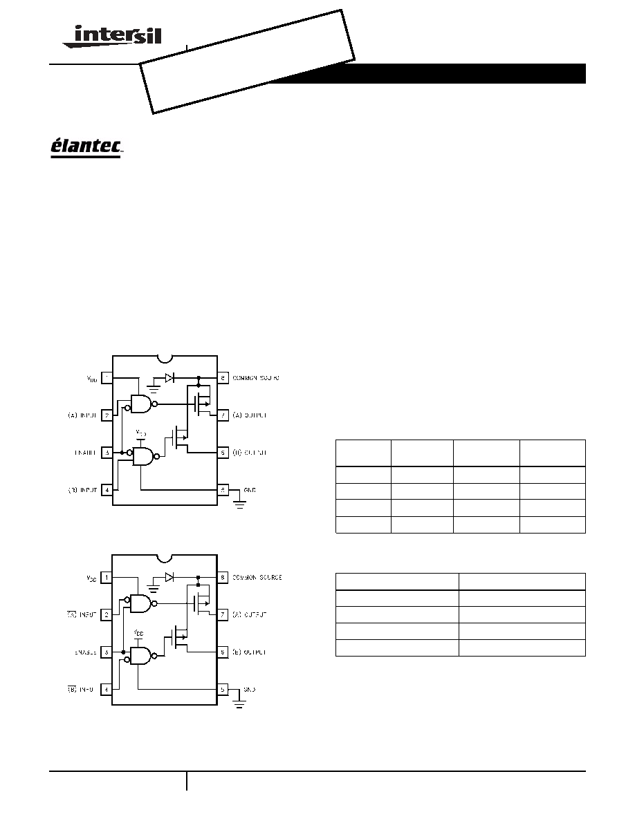
EL7240, EL7241
High Speed Coil Drivers
The EL7240/EL7241 high speed coil
drivers accept logic inputs which
independently control a pair of 3
PMOS FET's. The output transistors share a common
source, making these devices well suited for "current
steering" and analog switching applications. The typical
clamping diodes to ground are removed, thus allowing pins
(6) and (7) to swing negative. This feature is desirable when
driving "center-tapped" coils referenced to ground. The logic
"NAND" input configuration can be used to "enable" the
outputs. The EL7240 and EL7241 differ only by their logic
polarity.
Pinouts
Features
· 20ns Propagation delay
· Clock to 10MHz
· 2 Amp peak output drive
· 3
output impedance
· 3V/5V Logic input compatible
· Outputs "OK" below ground
· Operating voltage 4.5V to 16V
Applications
· Tape drive-write head driver
· Current switching
· Center-Tapped transformer driver
· ATE-pin drivers
· Analog switching
· AC switching
· T - switch
EL7240
(8-PIN PDIP, SOIC)
TOP VIEW
EL7241
(8-PIN PDIP, SOIC)
TOP VIEW
Ordering Information
PART
NUMBER
TEMP. RANGE
PACKAGE
PKG. NO.
EL7240CN
-40°C to +85°C
8-Pin PDIP
MDP0031
EL7240CS
-40°C to +85°C
8-Pin PSOIC
MDP0027
EL7241CN
-40°C to +85°C
8-Pin PDIP
MDP0031
EL7241CS
-40°C to +85°C
8-Pin PSOIC
MDP0027
Operating Voltage Range
PINS
MIN/MAX (VOLTS)
V
DD
/GND
4.5/16
V
DD
/Output
0/-20
Source/Output
0/-16
Output/GND
16/-10
Data Sheet
January 1996, Rev A
OBSO
LET
E PR
ODU
CT
NO R
ECO
MMEN
DED
REP
LAC
EMEN
T
cont
act o
ur T
echn
ical S
upp
ort C
ente
r at
1-88
8-IN
TER
SIL
or w
ww.
inter
sil.c
om/t
sc
2
Rise and Fall times (t
R
and t
F
) are load dependent.
Absolute Maximum Ratings
(T
A
= 25°C)
Supply (V+ to GND) . . . . . . . . . . . . . . . . . . . . . . . . . . . . . . . . . 16.5V
Input Pins . . . . . . . . . . . . . . . . . . . . . . . . . . -0.3V to +0.3V above V+
Combined Peak Output Current. . . . . . . . . . . . . . . . . . . . . . . . . . .4A
Storage Temperature Range . . . . . . . . . . . . . . . . . .-65°C to +150°C
Ambient Operating Temperature . . . . . . . . . . . . . . . . -40°C to +85°C
Operating Junction Temperature . . . . . . . . . . . . . . . . . . . . . . . 125°C
Power Dissipation
SOIC . . . . . . . . . . . . . . . . . . . . . . . . . . . . . . . . . . . . . . 570mW
PDIP . . . . . . . . . . . . . . . . . . . . . . . . . . . . . . . . . . . . . 1050mW
CAUTION: Stresses above those listed in "Absolute Maximum Ratings" may cause permanent damage to the device. This is a stress only rating and operation of the
device at these or any other conditions above those indicated in the operational sections of this specification is not implied.
IMPORTANT NOTE: All parameters having Min/Max specifications are guaranteed. Typical values are for information purposes only. Unless otherwise noted, all tests
are at the specified temperature and are pulsed tests, therefore: T
J
= T
C
= T
A
DC Electrical Specifications
T
A
= 25°C, V = 15V unless otherwise specified
PARAMETER
DESCRIPTION
TEST CONDITIONS
MIN
TYP
MAX
UNITS
INPUT
V
IH
Logic "1" Input Voltage
2.4
V
I
IH
Logic "1" Input Current
@V+
0.1
10
µA
V
IL
Logic "0" Input Voltage
0.8
V
I
IL
Logic "0" Input Current
@0V
0.1
10
µA
V
HVS
Input Hysteresis
0.3
V
OUTPUT
R
ON
Pull-Up Resistance
I
OUT
= -100mA
3
6
I
OFF
Off Leakage
V
OUT
= 0V
0.2
10
µA
I
PK
Peak Output Current
Source
2.0
A
I
DC
Continuous Output Current
Channel
100
mA
V
S
Source Potential with Grounded Drain
Channel A or B, 100mA Load
2.3
2.75
V
POWER SUPPLY
I
S
Power Supply Current
Inputs High
1
2.5
mA
V
S
Operating Voltage
4.5
16
V
AC Electrical Specifications
T
A
= 25°C, V = 15V unless otherwise specified
PARAMETER
DESCRIPTION
MIN
TYP
MAX
UNITS
SWITCHING CHARACTERISTICS
t
D-ON
Turn-On Delay Time
18
25
ns
t
D-OFF
Turn-Off Delay Time
20
25
ns
EL7240, EL7241
3
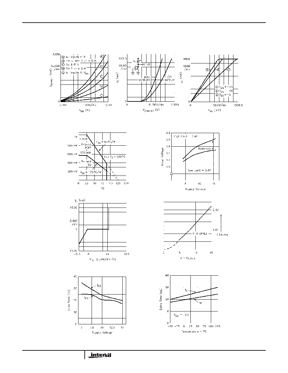
Typical Performance Curves
Supply Current vs V
DD
and Input
Connection
Source Voltage vs Current
(Grounded Drain )
Output Conduction vs V
GS
Max Power/Derating Curves
Switch Threshold vs Supply Voltage
Input Current vs Voltage
Propagation Delay vs Supply Voltage
Peak Drive vs Supply Voltage
Delay vs Temperature
EL7240, EL7241