1
®
FN7287.1
CAUTION: These devices are sensitive to electrostatic discharge; follow proper IC Handling Procedures.
1-888-INTERSIL or 321-724-7143
|
Intersil (and design) is a registered trademark of Intersil Americas Inc.
Copyright © Elantec Semiconductor, Inc. 1996, Intersil Americas Inc. 2004. All Rights Reserved. Elantec is a registered trademark of Elantec Semiconductor, Inc.
All other trademarks mentioned are the property of their respective owners.
EL7412
High Speed, Four Channel Power
MOSFET Drivers
The EL7412 contains (4) high performance matched drivers.
These very high speed drivers are capable of delivering
peak currents of 2.0 amps into highly capacitive loads and
are ideally suited for "Full bridge' and ultrasound
applications. The high speed performance is achieved by
means of a proprietary "Turbo-Driver' circuit that speeds up
input stages by tapping the wider voltage swing at the
output. Improved speed and drive capability are enhanced
by matched rise and fall delay times. The matched delays
maintain the integrity of input-to-output pulse-widths to
reduce timing errors and clock skew problems. This
improved performance is accompanied by a 10 fold
reduction in supply currents over bipolar drivers, yet without
the delay time problems commonly associated with CMOS
devices. Dynamic switching losses are minimized with non-
overlapped drive techniques.
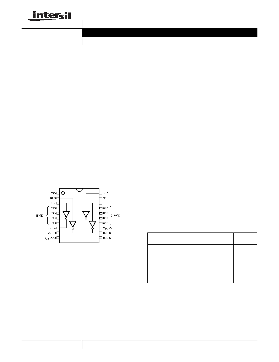
Pinout
Features
· Excellent response times
· Matched rise and fall times
· Reduced clock skew
· Low output impedance
· Low input capacitance
· High noise immunity
· Improved clocking rate
· Low supply current
· Wide operating voltage range
·
Pb-free available
Applications
· Full bridge drivers
· Clock/line drivers
· CCD Drivers
· Ultra-sound transducer drivers
· Power MOSFET drivers
· Switch mode power supplies
· Class D switching amplifiers
· Ultrasonic and RF generators
· Pulsed circuits
EL7412
[20-PIN SO (0.300")]
TOP VIEW
Note 1: Pins 47 and 1417 are electrically connected.
Manufactured under U.S. Patent Nos. 5,334,883, #5,331,047
Ordering Information
PART NUMBER
PACKAGE
TAPE &
REEL
PKG. DWG.
#
EL7412CM
20-Pin SO (0.300")
-
MDP0027
EL7412CM-T13
20-Pin SO (0.300")
13"
MDP0027
EL7412CMZ
(See Note)
20-Pin SO (0.300")
(Pb-free)
-
MDP0027
EL7412CMZ-
T13 (See Note)
20-Pin SO (0.300")
(Pb-free)
13"
MDP0027
NOTE: Intersil Pb-free products employ special Pb-free material
sets; molding compounds/die attach materials and 100% matte tin
plate termination finish, which is compatible with both SnPb and
Pb-free soldering operations. Intersil Pb-free products are MSL
classified at Pb-free peak reflow temperatures that meet or exceed
the Pb-free requirements of IPC/JEDEC J-Std-020C.
Data Sheet
August 26, 2004, Rev B
2
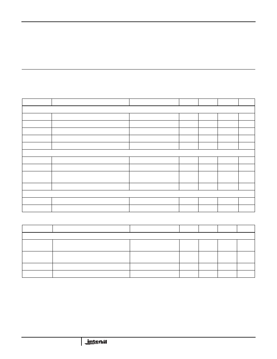
Absolute Maximum Ratings
(T
A
= 25°C)
Supply (V+ to Gnd) . . . . . . . . . . . . . . . . . . . . . . . . . . . . . . . . . 16.5V
Input Pins . . . . . . . . . . . . . . . . . . . . . . . . . . -0.3V to +0.3V above V+
Combined Peak Output Current. . . . . . . . . . . . . . . . . . . . . . . . . . .8A
Storage Temperature Range . . . . . . . . . . . . . . . . . .-65°C to +150°C
Ambient Operating Temperature . . . . . . . . . . . . . . . . -40°C to +85°C
Operating Junction Temperature . . . . . . . . . . . . . . . . . . . . . . . 125°C
Power Dissipation . . . . . . . . . . . . . . . . . . . . . . . . . . . . . See Curves
CAUTION: Stresses above those listed in "Absolute Maximum Ratings" may cause permanent damage to the device. This is a stress only rating and operation of the
device at these or any other conditions above those indicated in the operational sections of this specification is not implied.
IMPORTANT NOTE: All parameters having Min/Max specifications are guaranteed. Typical values are for information purposes only. Unless otherwise noted, all tests
are at the specified temperature and are pulsed tests, therefore: T
J
= T
C
= T
A
DC Electrical Specifications
T
A
= 25°C, V
DD
= 15V unless otherwise specified
PARAMETER
DESCRIPTION
TEST CONDITIONS
MIN
TYP
MAX
UNITS
INPUT
V
IH
Logic "1' Input Voltage
2.4
V
I
IH
Logic "1' Input Current
@V
DD
0.1
10
µA
V
IL
Logic "0' Input Voltage
0.8
V
I
IL
Logic "0' Input Current
@0V
0.1
10
µA
V
HVS
Input Hysteresis
0.3
V
OUTPUT
R
OH
Pull-Up Resistance
I
OUT
= -100mA
3
6
R
OL
Pull-Down Resistance
I
OUT
= +100mA
4
6
I
PK
Peak Output Current
Source
Sink
2
2
A
I
DC
Continuous Output Current
Source/Sink
100
mA
POWER SUPPLY
I
S
Power Supply Current
Inputs High
2
5
mA
V
S
Operating Voltage
4.5
15
V
AC Electrical Specifications
T
A
= 25°C, V = 15V unless otherwise specified
PARAMETER
DESCRIPTION
TEST CONDITIONS
MIN
TYP
MAX
UNITS
SWITCHING CHARACTERISTICS
t
R
Rise Time
C
L
= 500pF
C
L
= 1000pF
7.5
10
20
ns
t
F
Fall Time
C
L
= 500pF
C
L
= 1000pF
10
13
20
ns
t
D1
Turn-On Delay Time
See Timing Table
18
25
ns
t
D2
Turn-Off Delay Time
See Timing Table
20
25
ns
EL7412

4
Typical Performance Curves
Max Power/Derating Curves
Switch Threshold vs Supply Voltage
Input Current vs Voltage
"ON' Resistance vs Supply Voltage
Peak Drive vs Supply Voltage
Ambient Temperature (°C)
EL7412

5
Typical Performance Curves
(Continued)
Average Supply Current vs
Voltage and Frequency
Average Supply Current
vs Capacitive Load
Rise/Fall Time vs Load
Rise/Fall Time vs Supply Voltage
EL7412
