
1
July 1997
HA-2548/883
Precision, High Slew Rate,
Wideband Operational Amplifier
Features
∑ This Circuit is Processed in Accordance to MIL-STD-
883 and is Fully Conformant Under the Provisions of
Paragraph 1.2.1.
∑ High Slew Rate . . . . . . . . . . . . . . . . . . . . . 120V/
µ
s (Typ)
∑ Low Offset Voltage. . . . . . . . . . . . . . . . . . . . 300
µ
V (Typ)
900
µ
V (Max)
∑ High Open Loop Gain . . . . . . . . . . . . . . . . . 130dB (Typ)
114dB (Min)
∑ Gain Bandwidth Product . . . . . . . . . . . . . 150MHz (Typ)
∑ Low Voltage Noise at 1kHz . . . . . . . . . . 8.3nV/
Hz (Typ)
∑ Minimum Gain Stability . . . . . . . . . . . . . . . . . . .
5 (Typ)
Applications
∑ High Speed Instrumentation
∑ Data Acquisition Systems
∑ Analog Signal Conditioning
∑ Precision, Wideband Amplifiers
∑ Pulse/RF Amplifiers
Description
The HA-2548/883 is a monolithic op amp that offers a unique
combination of bandwidth, slew rate, and precision specifica-
tions. These features can eliminate the need for composite
op amp designs and external calibration circuitry.
Optimized for gains
5, the HA-2548/883 has a gain band-
width product of 150MHz (typ) and a slew rate of 120V/
µ
s
(typ) while maintaining an extremely high open loop gain of
130dB (typ) and a low offset voltage of 300
µ
V (typ). These
specifications are achieved through uniquely designed input
circuitry and a single ultra-high gain stage that minimizes the
AC signal path. Capable of delivering over 30mA (min) of
output current, the HA-2548/883 is ideal for precision, high
speed applications such as signal conditioning, instrumenta-
tion, video/pulse amplifiers and buffers.
Pinout
HA-2548/883
(METAL CAN)
TOP VIEW
Ordering Information
PART NUMBER
TEMP.
RANGE (
o
C)
PACKAGE
PKG.
NO.
HA2-2548/883
-55 to 125
8 Pin Can
T8.C
COMP
OUT
-IN
V -
+BAL
+IN
V+
-BAL
2
4
6
1
3
7
5
8
+
-
Spec Number
511069-883
File Number
2472.2
CAUTION: These devices are sensitive to electrostatic discharge; follow proper IC Handling Procedures.
1-888-INTERSIL or 321-724-7143 | Copyright © Intersil Corporation 1999
2
Spec Number
511069-883
Absolute Maximum Ratings
Thermal Information
Voltage Between V+ and V- Terminals . . . . . . . . . . . . . . . . . . . . 40V
Differential Input Voltage. . . . . . . . . . . . . . . . . . . . . . . . . . . . . . . . 5V
Voltage at Either Input Terminal . . . . . . . . . . . . . . . . . . . . . . V+ to V-
Peak Output Current (< 10% Duty Cycle). . . . . . . . . . . . . . . . . 60mA
Continuous Output Current. . . . . . . . . . . . . . . . . . . . . . . . . . . . 40mA
ESD Rating. . . . . . . . . . . . . . . . . . . . . . . . . . . . . . . . . . . . . . <2000V
Operating Conditions
Temperature Range . . . . . . . . . . . . . . . . . . . . . . . . . -55
o
C to 125
o
C
Supply Voltage
. . . . . . . . . . . . . . . . . . . . . . . . . . . . . . . . . . . . . . . . . ±
15V
V
INCM
1/2 (V+ - V-)
R
L
1k
Thermal Resistance (Typical, Note 1)
JA
JC
Metal Can Package . . . . . . . . . . . . . . .
142
o
C/W
66
o
C/W
Package Power Dissipation Limit at 75
o
C
Metal Can Package . . . . . . . . . . . . . . . . . . . . . . . . . . . . . . . 0.70W
Package Power Dissipation Derating Factor Above 75
o
C
Metal Can Package . . . . . . . . . . . . . . . . . . . . . . . . . . . . 7.0mW/
o
C
Maximum Junction Temperature . . . . . . . . . . . . . . . . . . . . . . . 175
o
C
Maximum Storage Temperature Range . . . . . . . . . .-65
o
C to 150
o
C
Maximum Lead Temperature (Soldering 10s) . . . . . . . . . . . . . 300
o
C
CAUTION: Stresses above those listed in "Absolute Maximum Ratings" may cause permanent damage to the device. This is a stress only rating and operation
of the device at these or any other conditions above those indicated in the operational sections of this specification is not implied.
NOTE:
1.
JA
is measured with the component mounted on an evaluation PC board in free air.
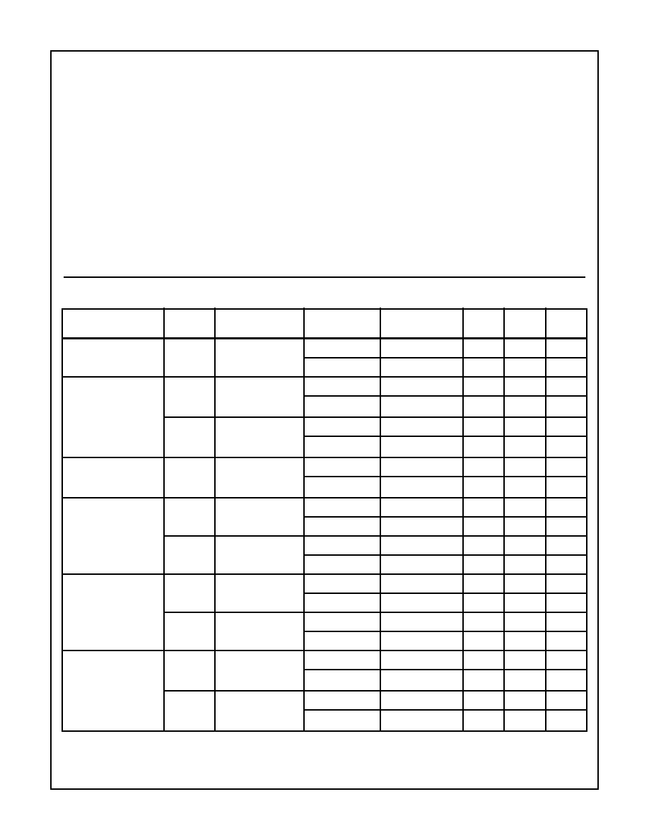
TABLE 1. DC ELECTRICAL PERFORMANCE CHARACTERISTICS
Device Tested at: V
SUPPLY
=
±
15V, R
LOAD
= 100k
, V
OUT
= 0V, Unless Otherwise Specified.
PARAMETERS
SYMBOL
CONDITIONS
GROUP A
SUBGROUPS
TEMP. (
o
C)
MIN
MAX
UNITS
Input Offset Voltage
V
IO
V
CM
= 0V
1
25
-900
900
µ
V
2, 3
125, -55
-1200
1200
µ
V
Input Bias Current
+I
B
V
CM
= 0V,
+R
S
= 100.1k
,
-R
S
= 100
1
25
-50
50
nA
2, 3
125, -55
-100
100
nA
-I
B
V
CM
= 0V,
+R
S
= 100
,
-R
S
= 100.1k
1
25
-50
50
nA
2, 3
125, -55
-100
100
nA
Input Offset Current
I
IO
V
CM
= 0V,
+R
S
= 100.1k
,
-R
S
= 100.1k
1
25
-50
50
nA
2, 3
125, -55
-100
100
nA
Common Mode Range
+CMR
V+ = +8V, V- = -22V
1
25
7
-
V
2, 3
125, -55
7
-
V
-CMR
V+ = +22V, V- = -8V
1
25
-
-7
V
2, 3
125, -55
-
-7
V
Large Signal Voltage
Gain
+A
VOL
V
OUT
= 0V and +10V,
R
L
= 1k
4
25
114
-
dB
5, 6
125, -55
108
-
dB
-A
VOL
V
OUT
= 0V and -10V,
R
L
= 1k
4
25
114
-
dB
5, 6
125, -55
108
-
dB
Common Mode
Rejection Ratio
+CMRR
V
CM
= +2V,
V+ = +13V, V- = -17V,
V
OUT
= -2V
1
25
80
-
dB
2, 3
125, -55
80
-
dB
-CMRR
V
CM
= -2V,
V+ = +17V, V- = -13V,
V
OUT
= 2V
1
25
80
-
dB
2, 3
125, -55
80
-
dB
HA-2548/883
3
Output Voltage Swing
+V
OUT
R
L
= 1k
4
25
11
-
V
5, 6
125, -55
11
-
V
-V
OUT
R
L
= 1k
4
25
-
-11
V
5, 6
125, -55
-
-11
V
Output Current
+I
OUT
V
OUT
= +10V
4
25
30
-
mA
5, 6
125, -55
30
-
mA
-I
OUT
V
OUT
= -10V
4
25
-
-30
mA
5, 6
125, -55
-
-30
mA
Quiescent Power Supply
Current
+I
CC
V
OUT
= 0V,
I
OUT
= 0mA
1
25
-
18
mA
2, 3
125, -55
-
18
mA
-I
CC
V
OUT
= 0V,
I
OUT
= 0mA
1
25
-18
-
mA
2, 3
125, -55
-18
-
mA
Power Supply
Rejection Ratio
+PSRR
V
SUP
= 10V,
V+ = +10V, V- = -15V,
V+ = +20V, V- = -15V
1
25
86
-
dB
2, 3
125, -55
86
-
dB
-PSRR
V
SUP
= 10V,
V+ = +15V, V- = -10V,
V+ = +15V, V- = -20V
1
25
86
-
dB
2, 3
125, -55
86
-
dB
TABLE 2. AC ELECTRICAL PERFORMANCE CHARACTERISTICS
Table 2 Intentionally Left Blank. See AC Characteristics in Table 3.
TABLE 3. ELECTRICAL PERFORMANCE CHARACTERISTICS
Device Characterized at: V
SUPPLY
=
±
15V, R
LOAD
= 1k
, C
LOAD
10pF, Unless Otherwise Specified.
PARAMETERS
SYMBOL
CONDITIONS
NOTES
TEMP. (
o
C)
MIN
MAX
UNITS
Average Offset Voltage Drift
V
IO
TC
V
CM
= 0V
2
-55 to 125
-
7
µ
V/
o
C
Offset Voltage Adjust
V
IO
Adj
2, 6
25
1
-
mV
Input Noise Voltage Density
EN
R
S
= 10
, f
O
= 1kHz
2
25
-
13.0
nV/
Hz
Input Noise Current Density
IN
R
S
= 500
, f
O
= 1kHz
2
25
-
1.0
pA/
Hz
Gain Bandwidth Product
GBWP
V
O
= 1.0V, f
O
= 1MHz
2
25
-
130
MHz
2
-55 to 125
-
110
MHz
Slew Rate
+SR
V
OUT
= -5V to +5V
2
25
80
-
V/
µ
s
2
-55 to 125
70
-
V/
µ
s
-SR
V
OUT
= +5V to -5V
2
25
80
-
V/
µ
s
2
-55 to 125
70
-
V/
µ
s
Full Power Bandwidth
FPBW
V
PEAK
= 10V
2, 3
25
1.11
-
MHz
TABLE 1. DC ELECTRICAL PERFORMANCE CHARACTERISTICS (Continued)
Device Tested at: V
SUPPLY
=
±
15V, R
LOAD
= 100k
, V
OUT
= 0V, Unless Otherwise Specified.
PARAMETERS
SYMBOL
CONDITIONS
GROUP A
SUBGROUPS
TEMP. (
o
C)
MIN
MAX
UNITS
HA-2548/883
Spec Number
511069-883
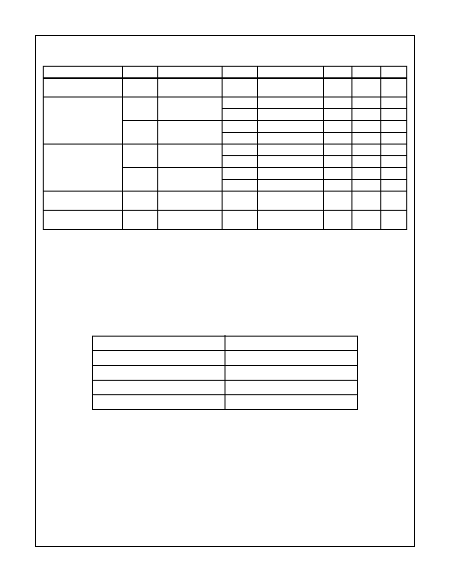
4
Spec Number
511069-883
Minimum Closed Loop
Stable Gain
CLSG
R
L
= 1k
, C
L
= 10pF
2
-55 to 125
5
-
V/V
Rise and Fall Time
t
r
V
OUT
= -100mV
to +100mV
2, 5
25
-
15
ns
2, 5
-55 to 125
-
20
ns
t
f
V
OUT
= +100mV
to -100mV
2, 5
25
-
15
ns
2, 5
-55 to 125
-
20
ns
Overshoot
+OS
V
OUT
= -100mV
to +100mV
2
25
-
30
%
2
-55 to 125
-
35
%
-OS
V
OUT
= +100mV
to -100mV
2
25
-
30
%
2
-55 to 125
-
35
%
Settling Time
t
S
To 0.01% for a 10V
Step
2
25
-
260
ns
Power Consumption
PC
V
OUT
= 0V,
I
OUT
= 0mA
2, 4
-55 to 125
-
540
mW
NOTES:
2. Parameters listed in Table 3 are controlled via design or process parameters and are not directly tested at final production. These param-
eters are lab characterized upon initial design release, or upon design changes. These parameters are guaranteed by characterization
based upon data from multiple production runs which reflect lot to lot and within lot variation.
3. Full Power Bandwidth guarantee based on Slew Rate measurement using FPBW = Slew Rate/(2
V
PEAK
).
4. Power Consumption based upon Quiescent Supply Current test maximum. (No load on outputs.)
5. Measured between 10% and 90% points.
6. Offset adjustment range is [V
IO
(Measured)
±
1mV] minimum referred to output. This test is for functionality only to assure adjustment
through 0V.
TABLE 4. ELECTRICAL TEST REQUIREMENTS
MIL-STD-883 TEST REQUIREMENTS
SUBGROUPS (SEE TABLE 1)
Interim Electrical Parameters (Pre Burn-In)
1
Final Electrical Test Parameters
1 (Note 7), 2, 3, 4, 5, 6
Group A Test Requirements
1, 2, 3, 4, 5, 6
Groups C and D Endpoints
1
NOTE:
7. PDA applies to Subgroup 1 only.
TABLE 3. ELECTRICAL PERFORMANCE CHARACTERISTICS (Continued)
Device Characterized at: V
SUPPLY
=
±
15V, R
LOAD
= 1k
, C
LOAD
10pF, Unless Otherwise Specified.
PARAMETERS
SYMBOL
CONDITIONS
NOTES
TEMP. (
o
C)
MIN
MAX
UNITS
HA-2548/883

5
Die Characteristics
DIE DIMENSIONS:
85 mils x 91 mils x 19 mils
2160
µ
m x 2320
µ
m x 483
µ
m
METALLIZATION:
Type: Al, 1% Cu
Thickness: 16k
≈
±
2k
≈
GLASSIVATION:
Type: Nitride (Si3N4) over Silox (SiO2, 5% Phos.)
Silox Thickness: 12k
≈
±
2k
≈
Nitride Thickness: 3.5k
≈
±
1.5k
≈
WORST CASE CURRENT DENSITY:
3.6 x 10
4
A/cm
2
SUBSTRATE POTENTIAL (Powered Up): V- (Note)
TRANSISTOR COUNT: 60
PROCESS: Bipolar, Dielectric Isolation
NOTE: The Substrate may be left floating (Insulating Die Mount) or it may be mounted on a conductor at a V- potential.
Metallization Mask Layout
HA-2548/883
+BAL
COMP
V+
OUT
V-
-BAL
-IN
+IN
HA-2548/883
Spec Number
511069-883

6
Spec Number
511069-883
Burn-In Circuit
HA2-2548/883 METAL CAN
NOTES:
R
1
= 1k
,
±
5%, 1/4W (Min)
R
2
= 1k
,
±
5%, 1/4W (Min)
R
3
= 10k
,
±
5%, 1/4W (Min)
C
1
= 0.01
µ
F/Socket or 0.1
µ
F/Row
C
2
= 0.01
µ
F/Socket or 0.1
µ
F/Row
D
1
= D
2
= 1N4002 or Equivalent/Board
|(V+) - (V-)| = 31V
±
1V
1
5
8
+
-
V+
C
1
D
1
6
2
7
3
R
2
4
C
2
D
2
V-
R
1
R
3
HA-2548/883
7
All Intersil semiconductor products are manufactured, assembled and tested under ISO9000 quality systems certification.
Intersil products are sold by description only. Intersil Corporation reserves the right to make changes in circuit design and/or specifications at any time without
notice. Accordingly, the reader is cautioned to verify that data sheets are current before placing orders. Information furnished by Intersil is believed to be accurate
and reliable. However, no responsibility is assumed by Intersil or its subsidiaries for its use; nor for any infringements of patents or other rights of third parties which
may result from its use. No license is granted by implication or otherwise under any patent or patent rights of Intersil or its subsidiaries.
For information regarding Intersil Corporation and its products, see web site http://www.intersil.com
Sales Office Headquarters
NORTH AMERICA
Intersil Corporation
P. O. Box 883, Mail Stop 53-204
Melbourne, FL 32902
TEL: (321) 724-7000
FAX: (321) 724-7240
EUROPE
Intersil SA
Mercure Center
100, Rue de la Fusee
1130 Brussels, Belgium
TEL: (32) 2.724.2111
FAX: (32) 2.724.22.05
ASIA
Intersil (Taiwan) Ltd.
Taiwan Limited
7F-6, No. 101 Fu Hsing North Road
Taipei, Taiwan
Republic of China
TEL: (886) 2 2716 9310
FAX: (886) 2 2715 3029
HA-2548/883
Spec Number
511069-883
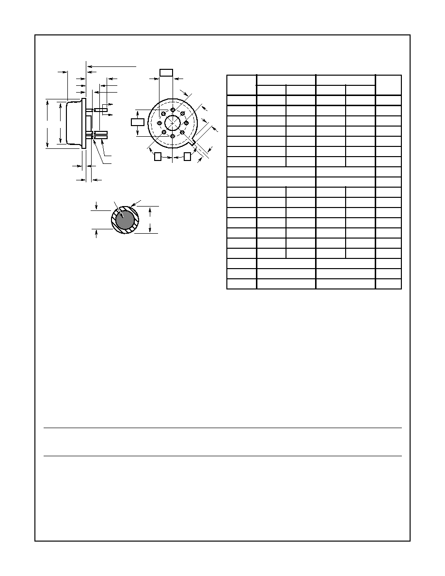
Metal Can Packages (Can)
NOTES:
1. (All leads) ÿb applies between L1 and L2. ÿb1 applies between
L2 and 0.500 from the reference plane. Diameter is uncontrolled
in L1 and beyond 0.500 from the reference plane.
2. Measured from maximum diameter of the product.
3.
is the basic spacing from the centerline of the tab to terminal 1
and
is the basic spacing of each lead or lead position (N -1
places) from
,
looking at the bottom of the package.
4. N is the maximum number of terminal positions.
5. Dimensioning and tolerancing per ANSI Y14.5M - 1982.
6. Controlling dimension: INCH.
ÿb
ÿD2
ÿ
e
k1
k
ÿb1
BASE AND
SEATING PLANE
F
Q
ÿD ÿD1
L1
L2
REFERENCE PLANE
L
A
ÿb2
ÿb1
BASE METAL
LEAD FINISH
SECTION A-A
A
A
N
e
1
C
L
2
1
T8.C
MIL-STD-1835 MACY1-X8 (A1)
8 LEAD METAL CAN PACKAGE
SYMBOL
INCHES
MILLIMETERS
NOTES
MIN
MAX
MIN
MAX
A
0.165
0.185
4.19
4.70
-
ÿb
0.016
0.019
0.41
0.48
1
ÿb1
0.016
0.021
0.41
0.53
1
ÿb2
0.016
0.024
0.41
0.61
-
ÿD
0.335
0.375
8.51
9.40
-
ÿD1
0.305
0.335
7.75
8.51
-
ÿD2
0.110
0.160
2.79
4.06
-
e
0.200 BSC
5.08 BSC
-
e1
0.100 BSC
2.54 BSC
-
F
-
0.040
-
1.02
-
k
0.027
0.034
0.69
0.86
-
k1
0.027
0.045
0.69
1.14
2
L
0.500
0.750
12.70
19.05
1
L1
-
0.050
-
1.27
1
L2
0.250
-
6.35
-
1
Q
0.010
0.045
0.25
1.14
-
45
o
BSC
45
o
BSC
3
45
o
BSC
45
o
BSC
3
N
8
8
4
Rev. 0 5/18/94