Document Outline
- HA-5004/883
- 100MHz Current Feedback Amplifier
- Description
- -55 to +125
- Pinout
- CAUTION: These devices are sensitive to electrostatic discharge. Users should follow proper IC Ha...
- Copyright © Harris Corporation 1998
- Absolute Maximum Ratings
- Thermal Information
- TABLE 1.� DC ELECTRICAL PERFORMANCE CHARACTERISTICS �
- VIO
- 1
- +25oC
- -2.5
- 2.5
- mV
- 2, 3
- +125oC, -55oC
- -20
- 20
- mV
- +IB
- 1
- +25oC
- -5
- 5
- mA
- 2, 3
- +125oC, -55oC
- -20
- 20
- mA
- SSGE
- 1
- +25oC
- -
- 0.43
- %
- 2, 3
- +125oC, -55oC
- -
- 0.75
- %
- LSGE1
- 1
- +25oC
- -
- 0.43
- %
- 2, 3
- +125oC, -55oC
- -
- 0.75
- %
- LSGE2
- 1
- +25oC
- -
- 0.43
- %
- 2, 3
- +125oC, -55oC
- -
- 0.75
- %
- AV
- 1
- +25oC
- 233
- -
- V/V
- 2, 3
- +125oC, -55oC
- 133
- -
- V/V
- AR
- 1
- +25oC
- 58
- -
- V/mA
- 2, 3
- +125oC, -55oC
- 33
- -
- V/mA
- ±VOUT1
- 1
- +25oC
- 11.5
- -11.5
- V
- 2, 3
- +125oC, -55oC
- 10.5
- -10.5
- V
- ±VOUT2
- 1
- +25oC
- 9.0
- -9.0
- V
- 2, 3
- +125oC, -55oC
- 8.0
- -8.0
- V
- ±IOUT
- 1
- +25oC
- 90
- -90
- mA
- 2, 3
- +125oC, -55oC
- 80
- -80
- mA
- VIH
- 1
- +25oC
- 2.0
- -
- V
- 2, 3
- +125oC, -55oC
- 2.0
- -
- V
- VIL
- 1
- +25oC
- -
- 0.8
- V
- 2, 3
- +125oC, -55oC
- -
- 0.8
- V
- PSRR1
- 1
- +25oC
- 50
- -
- dB
- 2, 3
- +125oC, -55oC
- 50
- -
- dB
- PSRR2
- 1
- +25oC
- 50
- -
- dB
- 2, 3
- +125oC, -55oC
- 50
- -
- dB
- +ICC
- 1
- +25oC
- -
- 16
- mA
- 2, 3
- +125oC, -55oC
- -
- 22
- mA
- -ICC
- 1
- +25oC
- -16
- -
- mA
- 2, 3
- +125oC, -55oC
- -22
- -
- mA
- TABLE 2.�AC ELECTRICAL PERFORMANCE CHARACTERISTICS
- TABLE 3.� ELECTRICAL PERFORMANCE CHARACTERISTICS �
- TABLE 4.�ELECTRICAL TEST REQUIREMENTS
- Die Characteristics
- Metallization Mask Layout
1
Æ
July 1998
HA-5004/883
100MHz Current Feedback Amplifier
Features
∑ This Circuit is Processed in Accordance to MIL-STD-
883 and is Fully Conformant Under the Provisions of
Paragraph 1.2.1.
∑ Slew Rate . . . . . . . . . . . . . . . . . . . . . . 1000V/
µ
s (Min)
1200V/
µ
s (Typ)
∑ Output Current . . . . . . . . . . . . . . . . . . . .
±
80mA (Min)
±
100mA (Typ)
∑ Drives . . . . . . . . . . . . . . . . . . .
±
8.0V into 100
(Min)
±
9.5V into 100
(Typ)
∑ V
SUPPLY
. . . . . . . . . . . . . . . . . . . . . . . . .
±
5V to
±
18V
∑ Thermal Overload Protection and Output Flag
∑ Bandwidth Nearly Independent of Gain
∑ Output Enable/Disable
Applications
∑ Unity Gain Video/Wideband Buffer
∑ Video Gain Block
∑ High Speed Peak Detector
∑ Fiber Optic Transmitters
∑ Zero Insertion Loss Transmission Line Drivers
∑ Current to Voltage Converter
∑ Radar Systems
Description
The HA-5004/883 current feedback amplifier is a video/wideband
amplifier optimized for low gain applications. The design is based
on current-mode feedback which allows the amplifier to achieve
higher closed loop bandwidth than voltage-mode feedback oper-
ational amplifiers. Since feedback is employed, the HA-5004/883
can offer better gain accuracy and lower distortion than open
loop buffers. Unlike conventional op amps, the bandwidth and
rise time of the HA-5004/883 are nearly independent of closed
loop gain. The 100MHz bandwidth at unity gain reduces to only
65MHz at a gain of 10. The HA-5004/883 may be used in place
of a conventional op amp with a significant improvement in speed
power product.
Several features have been designed in for added value. A ther-
mal overload feature protects the part against excessive junction
temperature by shutting down the output. If this feature is not
needed, it can be inhibited via a TTL input (TOI). A TTL chip
enable/disable (OE) input is also provided; when the chip is dis-
abled its output is high impedance. Finally, an open collector out-
put flag (TOL) is provided to indicate the status of the chip. The
status flag goes low to indicate when the chip is disabled due to
either the internal Thermal Overload shutdown or the external
disable.
In order to maximize bandwidth and output drive capacity, inter-
nal current limiting is not provided. However, current limiting may
be applied via the V
C
+ and V
C
- pins which provide power sepa-
rately to the output stage.
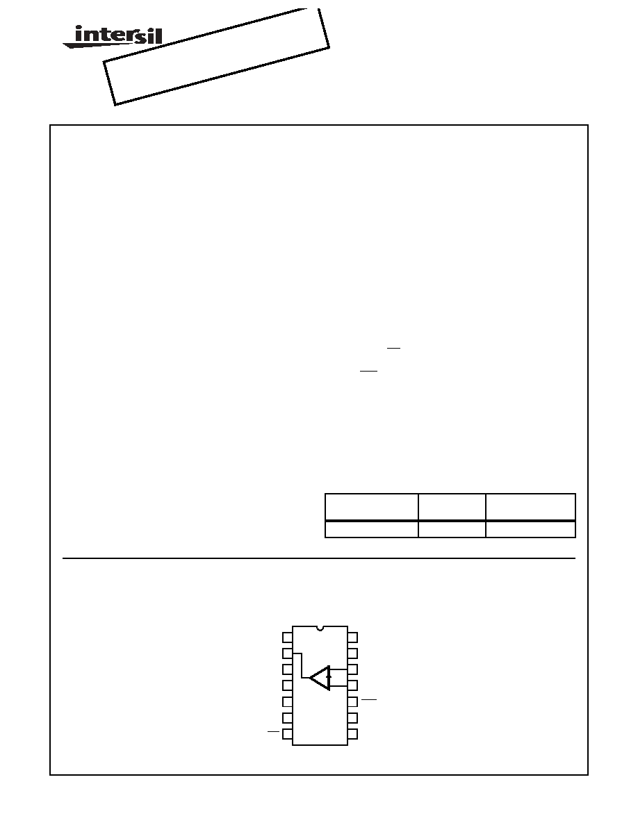
Pinout
HA-5004/883
(CERDIP)
TOP VIEW
Ordering Information
PART NUMBER
TEMP. RANGE
(
o
C)
PACKAGE
HA1-5004/883
-55 to +125
14 Lead CerDIP
OUT
TOI
OE
V
C
+
V+
+BAL
-BAL
FB
IN
TOL
GND
NC
V
C
-
V-
1
2
3
4
5
6
7
14
13
12
11
10
9
8
+
-
CAUTION: These devices are sensitive to electrostatic discharge. Users should follow proper IC Handling Procedures.
Copyright
©
Harris Corporation 1998
Spec Number
511053-883
File Number
3706.1
NOT
RECO
MME
NDED
FOR
NEW
DES
IGNS
conta
ct ou
r Tec
hnica
l Sup
port
Cent
er at
1-888
-INTE
RSIL
or w
ww.in
tersil
.com
/tsc
2
Absolute Maximum Ratings
Thermal Information
Voltage between V+ and V- Terminals. . . . . . . . . . . . . . . . . . . . 40V
Differential Input Voltage . . . . . . . . . . . . . . . . . . . . . . . . . . . . . . . 5V
Voltage at Either Input Terminal. . . . . . . . . . . . . . . . . . . . . . V+ to V-
Peak Output Current Pulsed at 1ms
10% Duty Cycle
. . . .±
3
0
0mA
Continuous Output Current
. . . . . . . . . . . . . . . . . . . . . . . . .±
120mA rms
Junction Temperature (T
J
) . . . . . . . . . . . . . . . . . . . . . . . . . . +175
o
C
Storage Temperature Range . . . . . . . . . . . . . . . . . -65
o
C to +150
o
C
ESD Rating. . . . . . . . . . . . . . . . . . . . . . . . . . . . . . . . . . . . . . <2000V
Lead Temperature (Soldering 10s). . . . . . . . . . . . . . . . . . . . +300
o
C
Thermal Resistance
JA
JC
CerDIP Package . . . . . . . . . . . . . . . . . . .
73
o
C/W
18
o
C/W
Package Power Dissipation Limit at +75
o
C
CerDIP Package . . . . . . . . . . . . . . . . . . . . . . . . . . . . . . . . . 1.37W
Package Power Dissipation Derating Factor Above +75
o
C
CerDIP Package . . . . . . . . . . . . . . . . . . . . . . . . . . . . . 13.7mW/
o
C
CAUTION: Stresses above those listed in "Absolute Maximum Ratings" may cause permanent damage to the device. This is a stress only rating and operation
of the device at these or any other conditions above those indicated in the operational sections of this specification is not implied.
Operating Conditions
Operating Temperature Range. . . . . . . . . . . . . . . . -55
o
C to +125
o
C
Operating Supply Voltage
. . . . . . . . . . . . . . . . . . . . . . . . . ±
12V to
±
15V
R
L
100
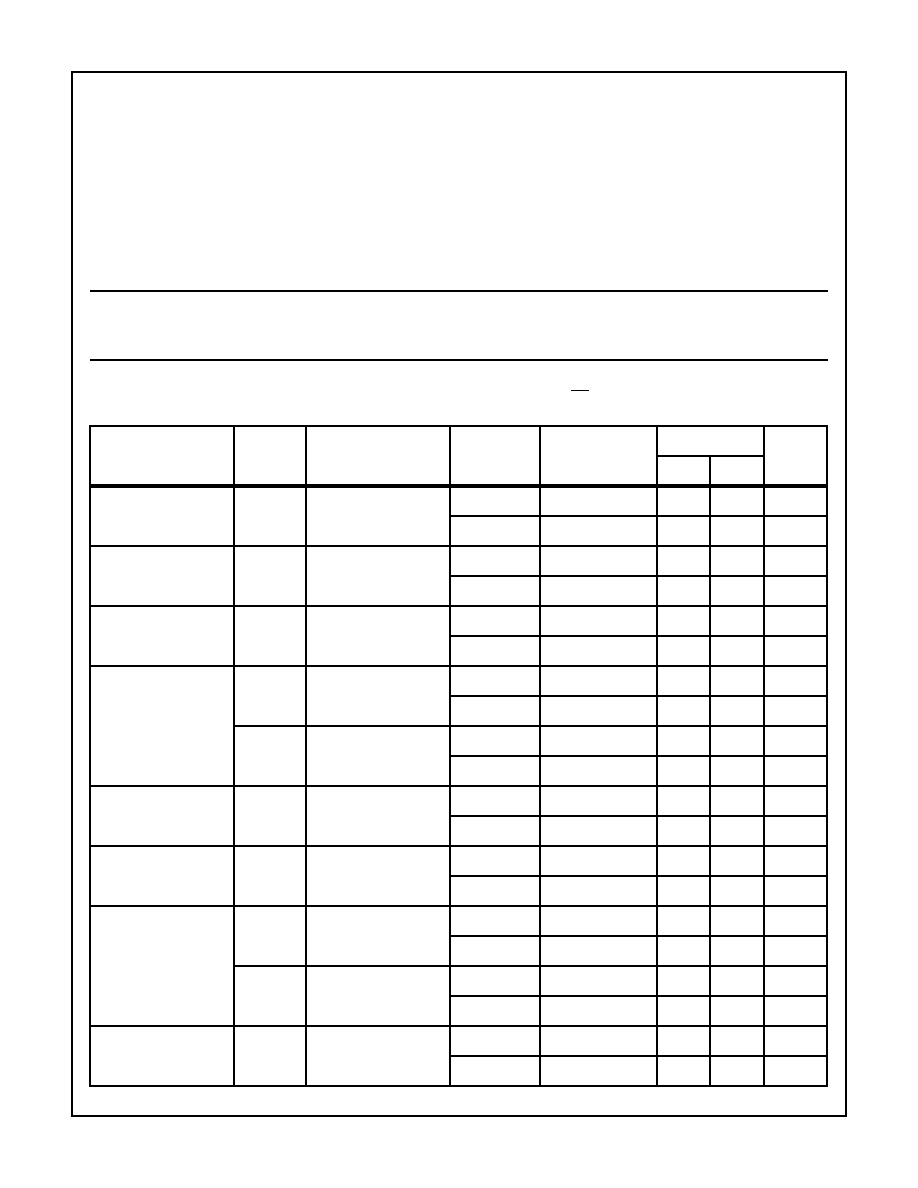
TABLE 1. DC ELECTRICAL PERFORMANCE CHARACTERISTICS
Device Tested at: V+ =
V
C
+
= +15V, V- =
V
C
- = -15V, R
L
= 100
, A
V
= +1, R
F
= 250
, OE = 0.8V, TOI = 0.8V or 2.0V,
Unless Otherwise Specified.
PARAMETERS
SYMBOL
CONDITIONS
GROUP A
SUBGROUP
TEMPERATURE
LIMITS
UNITS
MIN
MAX
Input Offset Voltage
V
IO
V
IN
= 0V
1
+25
o
C
-2.5
2.5
mV
2, 3
+125
o
C, -55
o
C
-20
20
mV
Input Bias Current
+I
B
V
IN
= 0V (Note 1)
1
+25
o
C
-5
5
µ
A
2, 3
+125
o
C, -55
o
C
-20
20
µ
A
DC Gain Error
(Small Signal)
SSGE
V
IN
=
±
100mV,
R
L
= 100
1
+25
o
C
-
0.43
%
2, 3
+125
o
C, -55
o
C
-
0.75
%
DC Gain Error
(Large Signal)
LSGE
1
V
IN
=
±
5.0V,
R
L
= 1k
1
+25
o
C
-
0.43
%
2, 3
+125
o
C, -55
o
C
-
0.75
%
LSGE
2
V
IN
=
±
10V,
R
L
= 1k
1
+25
o
C
-
0.43
%
2, 3
+125
o
C, -55
o
C
-
0.75
%
DC Voltage Gain
A
V
For All Gain Error
Conditions (Note 2)
1
+25
o
C
233
-
V/V
2, 3
+125
o
C, -55
o
C
133
-
V/V
DC Transimpedance
A
R
For All Gain Error
Conditions (Note 3)
1
+25
o
C
58
-
V/mA
2, 3
+125
o
C, -55
o
C
33
-
V/mA
Output Voltage Swing
±
V
OUT1
V
IN
=
±
15V,
R
L
= 1k
1
+25
o
C
11.5
-11.5
V
2, 3
+125
o
C, -55
o
C
10.5
-10.5
V
±
V
OUT2
V
IN
=
±
10V,
R
L
= 100
1
+25
o
C
9.0
-9.0
V
2, 3
+125
o
C, -55
o
C
8.0
-8.0
V
Output Current
±
I
OUT
V
IN
=
±
10V,
R
L
= 100
1
+25
o
C
90
-90
mA
2, 3
+125
o
C, -55
o
C
80
-80
mA
HA-5004/883
3
Logic Input Voltage
V
IH
Pins OE, TOI (Note 4)
1
+25
o
C
2.0
-
V
2, 3
+125
o
C, -55
o
C
2.0
-
V
V
IL
Pins OE, TOI
1
+25
o
C
-
0.8
V
2, 3
+125
o
C, -55
o
C
-
0.8
V
Power Supply
Rejection Ratio
PSRR
1
V+ = +10V, +20V
V- = -15V
1
+25
o
C
50
-
dB
2, 3
+125
o
C, -55
o
C
50
-
dB
PSRR
2
V- = -10V, -20V
V+ = +15V
1
+25
o
C
50
-
dB
2, 3
+125
o
C, -55
o
C
50
-
dB
Power Supply Current
+I
CC
V
IN
= 0V, R
L
= 1k
1
+25
o
C
-
16
mA
2, 3
+125
o
C, -55
o
C
-
22
mA
-I
CC
V
IN
= 0V, R
L
= 1k
1
+25
o
C
-16
-
mA
2, 3
+125
o
C, -55
o
C
-22
-
mA
NOTES:
1. Inverting (FB) input is a low impedance point; Bias Current and Offset Current are not specified for this terminal.
2. DC Voltage Gain =
, for all Gain Error conditions.
3. DC Transimpedance =
, R
F
= 250
, for all Gain Error conditions.
4. Please refer to the Truth Table in the Applications Information section.
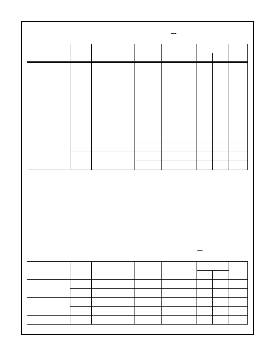
TABLE 2. AC ELECTRICAL PERFORMANCE CHARACTERISTICS
Table 2 Intentionally Left Blank. See AC Specifications in Table 3
TABLE 3. ELECTRICAL PERFORMANCE CHARACTERISTICS
Device Characterized at: V+ =
V
C
+ = +15V, V- =
V
C
- = -15V, R
L
= 1k
, A
V
= +1, R
F
= 250
, C
L
10pF, OE = 0.8V, TOI = 0.8V or 2.0V,
Unless Otherwise Specified.
PARAMETERS
SYMBOL
CONDITIONS
NOTES
TEMPERATURE
LIMITS
UNITS
MIN
MAX
Slew Rate
+SR
V
OUT
= 0V to +10V
1, 2
+25
o
C
1000
-
V/
µ
s
-SR
V
OUT
= 0V to -10V
1, 2
+25
o
C
1000
-
V/
µ
s
Rise and Fall Time
T
R
V
OUT
= 0V to +200mV,
1, 2
+25
o
C
-
7.0
ns
T
F
V
OUT
= 0V to -200mV
1, 2
+25
o
C
-
7.0
ns
Full Power Bandwidth
FPBW
V
PEAK
= 2V
1, 3
+25
o
C
79.5
-
MHz
TABLE 1. DC ELECTRICAL PERFORMANCE CHARACTERISTICS (Continued)
Device Tested at: V+ =
V
C
+
= +15V, V- =
V
C
- = -15V, R
L
= 100
, A
V
= +1, R
F
= 250
, OE = 0.8V, TOI = 0.8V or 2.0V,
Unless Otherwise Specified.
PARAMETERS
SYMBOL
CONDITIONS
GROUP A
SUBGROUP
TEMPERATURE
LIMITS
UNITS
MIN
MAX
1
Gain Error
---------------------------
RF
Gain Error
---------------------------
HA-5004/883
4
Quiescent Power
Consumption
PC
V
IN
= 0V
1, 4
-55
o
C to +125
o
C
-
660
mW
NOTES:
1. Parameters listed in Table 3 are controlled via design or process parameters and are not directly tested at final production. These param-
eters are lab characterized upon initial design release, or upon design changes. These parameters are guaranteed by characterization
based upon data from multiple production runs which reflect lot to lot and within lot variation.
2. Measured between 10% and 90% points.
3. Full Power Bandwidth guarantee based on Slew Rate measurement using FPBW = Slew Rate/(2
V
PEAK
).
4. Power Consumption based upon Quiescent Supply Current test maximum.
TABLE 3. ELECTRICAL PERFORMANCE CHARACTERISTICS (Continued)
Device Characterized at: V+ =
V
C
+ = +15V, V- =
V
C
- = -15V, R
L
= 1k
, A
V
= +1, R
F
= 250
, C
L
10pF, OE = 0.8V, TOI = 0.8V or 2.0V,
Unless Otherwise Specified.
PARAMETERS
SYMBOL
CONDITIONS
NOTES
TEMPERATURE
LIMITS
UNITS
MIN
MAX
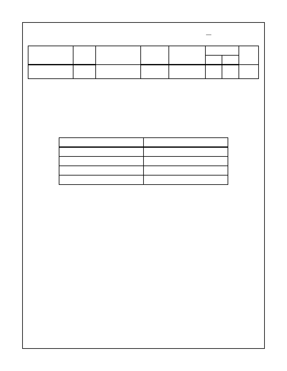
TABLE 4. ELECTRICAL TEST REQUIREMENTS
MIL-STD-883 TEST REQUIREMENTS
SUBGROUPS (SEE TABLE 1)
Interim Electrical Parameters (Pre Burn-In)
1
Final Electrical Test Parameters
1 (Note 1), 2, 3
Group A Test Requirements
1, 2, 3
Groups C & D Endpoints
1
NOTE:
1. PDA applies to Subgroup 1 only.
HA-5004/883
5
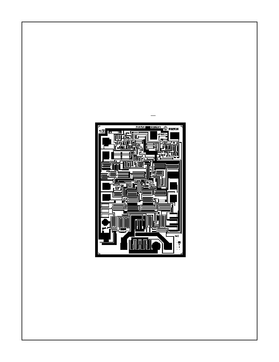
Die Characteristics
DIE DIMENSIONS:
63 x 93 x 19 mils
±
1 mils
1600 x 2370
x 483
µ
m
±
25.4
µ
m
METALLIZATION:
Type: Al, 1% Cu
Thickness: 16k
≈
±
2k
≈
GLASSIVATION:
Type: Nitride (Si3N4) over (Silox, 5% Phos.)
Silox Thickness: 12k
≈
±
2k
≈
Nitride Thickness: 3.5k
≈
±
1.5k
≈
WORST CASE CURRENT DENSITY:
6.6 x 10
4
A/cm
2
SUBSTRATE POTENTIAL (Powered Up): V
EE
TRANSISTOR COUNT: 64
PROCESS: Bipolar Dielectric Isolation
Metallization Mask Layout
HA-5004/883
OUT
VC+
VC-
V-
FB
IN
TOL
GND
OE
TOI
V+
-BAL
+BAL
HA-5004/883