
1
TM
HA5023
Dual 125MHz Video Current
Feedback Amplifier
The HA5023 is a wide bandwidth high slew rate dual
amplifier optimized for video applications and gains between
1 and 10. It is a current feedback amplifier and thus yields
less bandwidth degradation at high closed loop gains than
voltage feedback amplifiers.
The low differential gain and phase, 0.1dB gain flatness, and
ability to drive two back terminated 75
cables, make this
amplifier ideal for demanding video applications.
The current feedback design allows the user to take
advantage of the amplifier's bandwidth dependency on the
feedback resistor. By reducing R
F
, the bandwidth can be
increased to compensate for decreases at higher closed
loop gains or heavy output loads.
The performance of the HA5023 is very similar to the
popular Intersil HA-5020
.
Features
∑ Wide Unity Gain Bandwidth . . . . . . . . . . . . . . . . . 125MHz
∑ Slew Rate. . . . . . . . . . . . . . . . . . . . . . . . . . . . . . . 475V/
µ
s
∑ Input Offset Voltage . . . . . . . . . . . . . . . . . . . . . . . . 800
µ
V
∑ Differential Gain . . . . . . . . . . . . . . . . . . . . . . . . . . . 0.03%
∑ Differential Phase. . . . . . . . . . . . . . . . . . . . . 0.03 Degrees
∑ Supply Current (per Amplifier) . . . . . . . . . . . . . . . . 7.5mA
∑ ESD Protection. . . . . . . . . . . . . . . . . . . . . . . . . . . . 4000V
∑ Guaranteed Specifications at
±
5V Supplies
Applications
∑ Video Gain Block
∑ Video Distribution Amplifier/RGB Amplifier
∑ Flash A/D Driver
∑ Current to Voltage Converter
∑ Medical Imaging
∑ Radar and Imaging Systems
∑ Video Switching and Routing
Pinout
HA5023
(PDIP, SOIC)
TOP VIEW
Ordering Information
PART NUMBER
(BRAND)
TEMP.
RANGE (
o
C)
PACKAGE
PKG.
NO.
HA5023IP
-40 to 85
8 Ld PDIP
E8.3
HA5023IB
(H5023I)
-40 to 85
8 Ld SOIC
M8.15
HA5023EVAL
High Speed Op Amp DIP Evaluation Board
OUT1
-IN1
+IN1
V-
1
2
3
4
8
7
6
5
V+
OUT2
-IN2
+IN2
+
-
+
-
Data Sheet
September 1998
FN3393.6
CAUTION: These devices are sensitive to electrostatic discharge; follow proper IC Handling Procedures.
1-888-INTERSIL or 321-724-7143
|
Intersil (and design) is a trademark of Intersil Americas Inc.
Copyright © Intersil Americas Inc. 2002. All Rights Reserved

2
Absolute Maximum Ratings
Thermal Information
Voltage Between V+ and V- Terminals . . . . . . . . . . . . . . . . . . . .36V
DC Input Voltage (Note 3) . . . . . . . . . . . . . . . . . . . . . . . .
±
V
SUPPLY
Differential Input Voltage . . . . . . . . . . . . . . . . . . . . . . . . . . . . . . .10V
Output Current (Note 4) . . . . . . . . . . . . . . . . .Short Circuit Protected
ESD Rating (Note 3)
Human Body Model (Per MIL-STD-883 Method 3015.7). . . 2000V
Operating Conditions
Temperature Range. . . . . . . . . . . . . . . . . . . . . . . . . . -40
o
C to 85
o
C
Supply Voltage Range (Typical) . . . . . . . . . . . . . . . .
±
4.5V to
±
15V
Thermal Resistance (Typical, Note 2)
JA
(
o
C/W)
PDIP Package . . . . . . . . . . . . . . . . . . . . . . . . . . . . .
130
SOIC Package . . . . . . . . . . . . . . . . . . . . . . . . . . . . .
160
Maximum Junction Temperature (Note 1) . . . . . . . . . . . . . . . . .175
o
C
Maximum Junction Temperature (Plastic Package, Note 1) . . 150
o
C
Maximum Storage Temperature Range . . . . . . . . . -65
o
C to 150
o
C
Maximum Lead Temperature (Soldering 10s) . . . . . . . . . . . . 300
o
C
(SOIC - Lead Tips Only)
CAUTION: Stresses above those listed in "Absolute Maximum Ratings" may cause permanent damage to the device. This is a stress only rating and operation of the
device at these or any other conditions above those indicated in the operational sections of this specification is not implied.
NOTES:
1. Maximum power dissipation, including output load, must be designed to maintain junction temperature below 175
o
C for die, and below 150
o
C
for plastic packages. See Application Information section for safe operating area information.
2.
JA
is measured with the component mounted on an evaluation PC board in free air.
3. The non-inverting input of unused amplifiers must be connected to GND.
4. Output is protected for short circuits to ground. Brief short circuits to ground will not degrade reliability, however, continuous (100% duty cycle)
output current should not exceed 15mA for maximum reliability.
Electrical Specifications
V
SUPPLY
=
±
5V, R
F
= 1k
,
A
V
= +1, R
L
= 400
,
C
L
10pF,
Unless Otherwise Specified
PARAMETER
TEST CONDITIONS
(NOTE 9)
TEST
LEVEL
TEMP.
(
o
C)
MIN
TYP
MAX
UNITS
INPUT CHARACTERISTICS
Input Offset Voltage (V
IO
)
A
25
-
0.8
3
mV
A
Full
-
-
5
mV
Delta V
IO
Between Channels
A
Full
-
1.2
3.5
mV
Average Input Offset Voltage Drift
B
Full
-
5
-
µ
V/
o
C
V
IO
Common Mode Rejection Ratio
Note 5
A
25
53
-
-
dB
A
Full
50
-
-
dB
V
IO
Power Supply Rejection Ratio
±
3.5V
V
S
±
6.5V
A
25
60
-
-
dB
A
Full
55
-
-
dB
Input Common Mode Range
Note 5
A
Full
±
2.5
-
-
V
Non-Inverting Input (+IN) Current
A
25
-
3
8
µ
A
A
Full
-
-
20
µ
A
+IN Common Mode Rejection
(+I
BCMR
=
)
Note 5
A
25
-
-
0.15
µ
A/V
A
Full
-
-
0.5
µ
A/V
+IN Power Supply Rejection
±
3.5V
V
S
±
6.5V
A
25
-
-
0.1
µ
A/V
A
Full
-
-
0.3
µ
A/V
Inverting Input (-IN) Current
A
25, 85
-
4
12
µ
A
A
-40
-
10
30
µ
A
Delta -IN BIAS Current Between Channels
A
25, 85
-
6
15
µ
A
A
-40
-
10
30
µ
A
1
+R
IN
HA5023
3
-IN Common Mode Rejection
Note 5
A
25
-
-
0.4
µ
A/V
A
Full
-
-
1.0
µ
A/V
-IN Power Supply Rejection
±
3.5V
V
S
±
6.5V
A
25
-
-
0.2
µ
A/V
A
Full
-
-
0.5
µ
A/V
Input Noise Voltage
f = 1kHz
B
25
-
4.5
-
nV/
Hz
+Input Noise Current
f = 1kHz
B
25
-
2.5
-
pA/
Hz
-Input Noise Current
f = 1kHz
B
25
-
25.0
-
pA/
Hz
TRANSFER CHARACTERISTICS
Transimpedence
Note 11
A
25
1.0
-
-
M
A
Full
0.85
-
-
M
Open Loop DC Voltage Gain
R
L
= 400
, V
OUT
=
±
2.5V
A
25
70
-
-
dB
A
Full
65
-
-
dB
Open Loop DC Voltage Gain
R
L
= 100
, V
OUT
=
±
2.5V
A
25
50
-
-
dB
A
Full
45
-
-
dB
OUTPUT CHARACTERISTICS
Output Voltage Swing
R
L
= 150
A
25
±
2.5
±
3.0
-
V
A
Full
±
2.5
±
3.0
-
V
Output Current
R
L
= 150
B
Full
±
16.6
±
20.0
-
mA
Output Current, Short Circuit
V
IN
=
±
2.5V, V
OUT
= 0V
A
Full
±
40
±
60
-
mA
POWER SUPPLY CHARACTERISTICS
Supply Voltage Range
A
25
5
-
15
V
Quiescent Supply Current
A
Full
-
7.5
10
mA/Op Amp
AC CHARACTERISTICS (A
V
= +1)
Slew Rate
Note 6
B
25
275
350
-
V/
µ
s
Full Power Bandwidth
Note 7
B
25
22
28
-
MHz
Rise Time
Note 8
B
25
-
6
-
ns
Fall Time
Note 8
B
25
-
6
-
ns
Propagation Delay
Note 8
B
25
-
6
-
ns
Overshoot
B
25
-
4.5
-
%
-3dB Bandwidth
V
OUT
= 100mV
B
25
-
125
-
MHz
Settling Time to 1%
2V Output Step
B
25
-
50
-
ns
Settling Time to 0.25%
2V Output Step
B
25
-
75
-
ns
Electrical Specifications
V
SUPPLY
=
±
5V, R
F
= 1k
,
A
V
= +1, R
L
= 400
,
C
L
10pF,
Unless Otherwise Specified
(Continued)
PARAMETER
TEST CONDITIONS
(NOTE 9)
TEST
LEVEL
TEMP.
(
o
C)
MIN
TYP
MAX
UNITS
HA5023
4
AC CHARACTERISTICS (A
V
= +2, R
F
= 681
)
Slew Rate
Note 6
B
25
-
475
-
V/
µ
s
Full Power Bandwidth
Note 7
B
25
-
26
-
MHz
Rise Time
Note 8
B
25
-
6
-
ns
Fall Time
Note 8
B
25
-
6
-
ns
Propagation Delay
Note 8
B
25
-
6
-
ns
Overshoot
B
25
-
12
-
%
-3dB Bandwidth
V
OUT
= 100mV
B
25
-
95
-
MHz
Settling Time to 1%
2V Output Step
B
25
-
50
-
ns
Settling Time to 0.25%
2V Output Step
B
25
-
100
-
ns
Gain Flatness
5MHz
B
25
-
0.02
-
dB
20MHz
B
25
-
0.07
-
dB
AC CHARACTERISTICS (A
V
= +10, R
F
= 383
)
Slew Rate
Note 6
B
25
350
475
-
V/
µ
s
Full Power Bandwidth
Note 7
B
25
28
38
-
MHz
Rise Time
Note 8
B
25
-
8
-
ns
Fall Time
Note 8
B
25
-
9
-
ns
Propagation Delay
Note 8
B
25
-
9
-
ns
Overshoot
B
25
-
1.8
-
%
-3dB Bandwidth
V
OUT
= 100mV
B
25
-
65
-
MHz
Settling Time to 1%
2V Output Step
B
25
-
75
-
ns
Settling Time to 0.1%
2V Output Step
B
25
-
130
-
ns
VIDEO CHARACTERISTICS
Differential Gain (Note 10)
R
L
= 150
B
25
-
0.03
-
%
Differential Phase (Note 10)
R
L
= 150
B
25
-
0.03
-
Degrees
NOTES:
5. V
CM
=
±
2.5V. At -40
o
C Product is tested at V
CM
=
±
2.25V because Short Test Duration does not allow self heating.
6. V
OUT
switches from -2V to +2V, or from +2V to -2V. Specification is from the 25% to 75% points.
7.
.
8. R
L
= 100
, V
OUT
= 1V. Measured from 10% to 90% points for rise/fall times; from 50% points of input and output for propagation delay.
9. A. Production Tested; B. Typical or Guaranteed Limit based on characterization; C. Design Typical for information only.
10. Measured with a VM700A video tester using an NTC-7 composite VITS.
11. V
OUT
=
±
2.5V. At -40
o
C Product is tested at V
OUT
=
±
2.25V because Short Test Duration does not allow self heating.
Electrical Specifications
V
SUPPLY
=
±
5V, R
F
= 1k
,
A
V
= +1, R
L
= 400
,
C
L
10pF,
Unless Otherwise Specified
(Continued)
PARAMETER
TEST CONDITIONS
(NOTE 9)
TEST
LEVEL
TEMP.
(
o
C)
MIN
TYP
MAX
UNITS
FPBW
Slew Rate
2
VPEAK
-----------------------------
; VPEAK 2V
=
=
HA5023
5
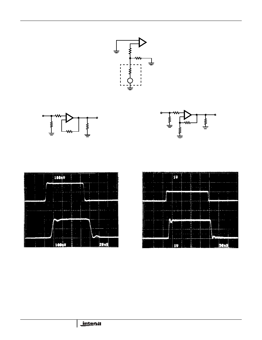
Test Circuits and Waveforms
FIGURE 1. TEST CIRCUIT FOR TRANSIMPEDANCE MEASUREMENTS
FIGURE 2. SMALL SIGNAL PULSE RESPONSE CIRCUIT
FIGURE 3. LARGE SIGNAL PULSE RESPONSE CIRCUIT
NOTE:
12. A series input resistor of
100
is recommended to limit input currents in case input signals are present before the HA5023 is powered up.
FIGURE 4. SMALL SIGNAL RESPONSE
FIGURE 5. LARGE SIGNAL RESPONSE
+
-
50
50
DUT
HP4195
NETWORK
ANALYZER
V
IN
V
OUT
R
L
R
F
, 1k
100
50
+
-
DUT
100
(NOTE 12)
V
IN
V
OUT
R
L
R
F
, 681
400
50
+
-
DUT
R
I
681
100
(NOTE 12)
Vertical Scale: V
IN
= 100mV/Div., V
OUT
= 100mV/Div.
Horizontal Scale: 20ns/Div.
Vertical Scale: V
IN
= 1V/Div., V
OUT
= 1V/Div.
Horizontal Scale: 50ns/Div.
HA5023
6
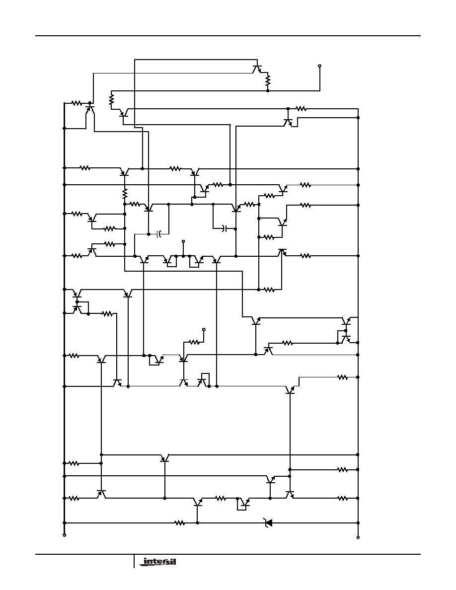
Schematic Diagram
(One Amplifier of Two)
R
2
800
R
5
2.5K
Q
P2
R
1
60K
Q
N1
R
3
6K
Q
N2
D
1
Q
N3
Q
N4
R
4
800
Q
N7
R
9
820
Q
P4
Q
N6
Q
N5
+IN
Q
P7
R
13
1K
R
12
280
Q
P6
Q
N8
Q
P5
R
10
820
Q
N9
Q
N11
Q
N10
Q
P10
Q
P8
Q
P9
R
11
1K
R
14
280
Q
N14
R
16
400
R
22
280
Q
N16
R
17
280
R
18
280
Q
P11
R
15
400
R
19
400
Q
P14
Q
N12
Q
P12
-IN
Q
N13
Q
P13
C
2
R
23
400
R
26
200
R
24
140
R
20
140
Q
P15
C
1
Q
N17
R
25
20
Q
N18
R
25
140
R
21
140
Q
P16
R
27
200
Q
P17
R
28
20
Q
N15
R
30
7
Q
N19
OUT
Q
N21
R
32
5
R
29
9.5
Q
P19
Q
P20
R
31
5
V+
V-
Q
P1
R
33
800
1.4pF
1.4pF
H
A
5
023
7
Application Information
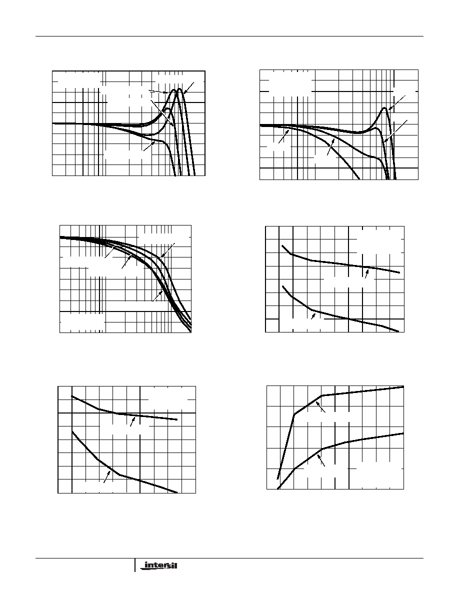
Optimum Feedback Resistor
The plots of inverting and non-inverting frequency response,
see Figure 8 and Figure 9 in the typical performance section,
illustrate the performance of the HA5023 in various closed
loop gain configurations. Although the bandwidth
dependency on closed loop gain isn't as severe as that of a
voltage feedback amplifier, there can be an appreciable
decrease in bandwidth at higher gains. This decrease may
be minimized by taking advantage of the current feedback
amplifier's unique relationship between bandwidth and R
F
.
All current feedback amplifiers require a feedback resistor,
even for unity gain applications, and R
F
, in conjunction with
the internal compensation capacitor, sets the dominant pole
of the frequency response. Thus, the amplifier's bandwidth is
inversely proportional to R
F
. The HA5023 design is
optimized for a 1000
R
F
at a gain of +1. Decreasing R
F
in
a unity gain application decreases stability, resulting in
excessive peaking and overshoot. At higher gains the
amplifier is more stable, so R
F
can be decreased in a trade-
off of stability for bandwidth.
The table below lists recommended R
F
values for various
gains, and the expected bandwidth.
PC Board Layout
The frequency response of this amplifier depends greatly on
the amount of care taken in designing the PC board. The
use of low inductance components such as chip resistors
and chip capacitors is strongly recommended. If leaded
components are used the leads must be kept short
especially for the power supply decoupling components and
those components connected to the inverting input.
Attention must be given to decoupling the power supplies. A
large value (10
µ
F) tantalum or electrolytic capacitor in
parallel with a small value (0.1
µ
F) chip capacitor works well
in most cases.
A ground plane is strongly recommended to control noise.
Care must also be taken to minimize the capacitance to
ground seen by the amplifier's inverting input (-IN). The
larger this capacitance, the worse the gain peaking, resulting
in pulse overshoot and possible instability. It is
recommended that the ground plane be removed under
traces connected to -IN, and that connections to -IN be kept
as short as possible to minimize the capacitance from this
node to ground.
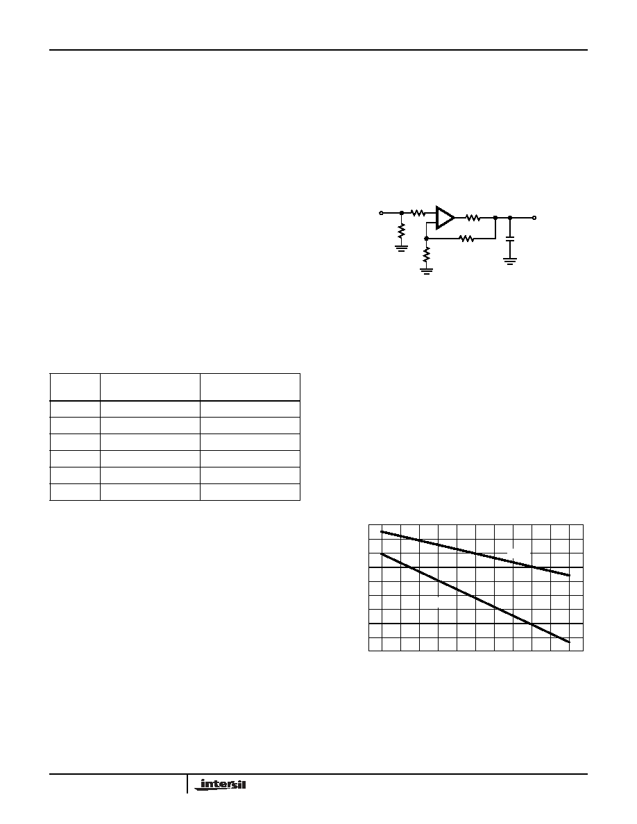
Driving Capacitive Loads
Capacitive loads will degrade the amplifier's phase margin
resulting in frequency response peaking and possible
oscillations. In most cases the oscillation can be avoided by
placing an isolation resistor (R) in series with the output as
shown in Figure 6.
The selection criteria for the isolation resistor is highly
dependent on the load, but 27
has been determined to be
a good starting value.
Power Dissipation Considerations
Due to the high supply current inherent in dual amplifiers, care
must be taken to insure that the maximum junction
temperature (T
J
,
see Absolute Maximum Ratings) is not
exceeded. Figure 7 shows the maximum ambient
temperature versus supply voltage for the available package
styles (Plastic DIP, SOIC). At
±
5V
DC
quiescent operation both
package styles may be operated over the full industrial range
of -40
o
C to 85
o
C. It is recommended that thermal
calculations, which take into account output power, be
performed by the designer.
GAIN
(A
CL
)
R
F
(
)
BANDWIDTH
(MHz)
-1
750
100
+1
1000
125
+2
681
95
+5
1000
52
+10
383
65
-10
750
22
V
IN
V
OUT
C
L
R
T
+
-
R
I
R
F
R
FIGURE 6. PLACEMENT OF THE OUTPUT ISOLATION
RESISTOR, R
100
5
7
9
11
13
15
140
130
120
110
100
90
80
SUPPLY VOLTAGE (
±
V)
PDIP
SOIC
M
A
X
AM
BI
E
N
T
T
E
M
P
E
RAT
URE
(
o
C)
50
60
70
FIGURE 7. MAXIMUM OPERATING AMBIENT TEMPERATURE
vs SUPPLY VOLTAGE
HA5023
8
Typical Performance Curves
V
SUPPLY
=
±
5V, A
V
= +1, R
F
= 1k
,
R
L
= 400
,
T
A
= 25
o
C,
Unless Otherwise Specified
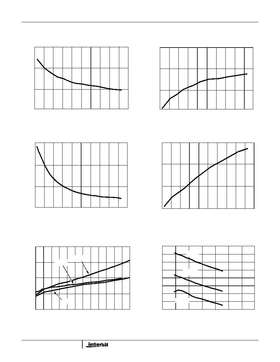
FIGURE 8. NON-INVERTING FREQENCY RESPONSE
FIGURE 9. INVERTING FREQUENCY RESPONSE
FIGURE 10. PHASE RESPONSE AS A FUNCTION OF
FREQUENCY
FIGURE 11. BANDWIDTH AND GAIN PEAKING vs FEEDBACK
RESISTANCE
FIGURE 12. BANDWIDTH AND GAIN PEAKING vs FEEDBACK
RESISTANCE
FIGURE 13. BANDWIDTH AND GAIN PEAKING vs LOAD
RESISTANCE
5
4
3
2
1
0
-1
-2
-3
-4
-5
NO
RM
AL
IZ
E
D
G
A
IN (
d
B)
FREQUENCY (MHz)
2
10
100
200
V
OUT
= 0.2V
P-P
C
L
= 10pF
A
V
= +1, R
F
= 1k
A
V
= 2, R
F
= 681
A
V
= 5, R
F
= 1k
A
V
= 10, R
F
= 383
5
4
3
2
1
0
-1
-2
-3
-4
-5
2
10
100
200
FREQUENCY (MHz)
N
O
RM
AL
IZ
E
D
G
A
IN
(
d
B)
V
OUT
= 0.2V
P-P
C
L
= 10pF
R
F
= 750
A
V
= -1
A
V
= -2
A
V
= -10
A
V
= -5
FREQUENCY (MHz)
2
10
100
200
0
-45
-90
-135
-100
-225
-270
-315
-360
180
135
90
0
-45
-90
-135
45
-180
NO
NINV
E
R
T
I
NG
P
HAS
E
(
D
E
G
RE
E
S
)
INV
E
RT
ING
P
HAS
E
(
D
E
G
RE
E
S
)
V
OUT
= 0.2V
P-P
C
L
= 10pF
A
V
= +10, R
F
= 383
A
V
= -10, R
F
= 750
A
V
= -1, R
F
= 750
A
V
= +1, R
F
= 1k
FEEDBACK RESISTOR (
)
500
700
900
1100
1300
1500
140
130
120
10
5
0
-
3
d
B
BANDW
IDT
H
(
M
Hz
)
G
A
IN P
E
AKING
(
d
B)
V
OUT
= 0.2V
P-P
C
L
= 10pF
-3dB BANDWIDTH
GAIN PEAKING
A
V
= +1
FEEDBACK RESISTOR (
)
-
3
d
B
BANDW
IDT
H
(
M
Hz
)
G
A
IN P
E
AKING
(
d
B)
100
95
90
0
350
500
650
800
950
1100
-3dB BANDWIDTH
GAIN PEAKING
V
OUT
= 0.2V
P-P
C
L
= 10pF
A
V
= +2
5
10
LOAD RESISTOR (
)
-
3
d
B
BANDW
IDT
H
(
M
Hz
)
G
A
IN
P
E
A
K
I
NG
(
d
B)
130
120
110
100
90
80
0
200
400
600
800
1000
6
4
2
0
V
OUT
= 0.2V
P-P
C
L
= 10pF
-3dB BANDWIDTH
GAIN PEAKING
A
V
= +1
HA5023
9
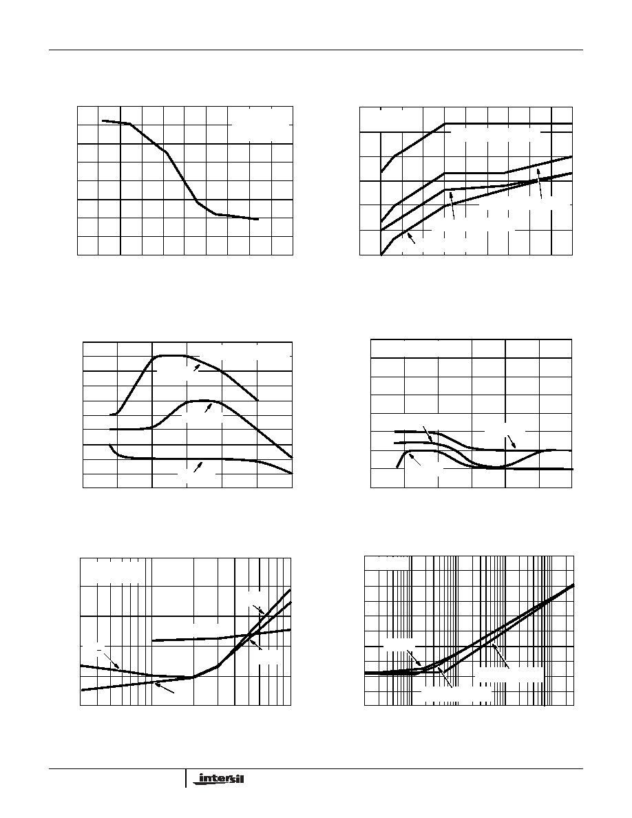
FIGURE 14. BANDWIDTH vs FEEDBACK RESISTANCE
FIGURE 15. SMALL SIGNAL OVERSHOOT vs LOAD
RESISTANCE
FIGURE 16. DIFFERENTIAL GAIN vs SUPPLY VOLTAGE
FIGURE 17. DIFFERENTIAL PHASE vs SUPPLY VOLTAGE
FIGURE 18. DISTORTION vs FREQUENCY
FIGURE 19. REJECTION RATIOS vs FREQUENCY
Typical Performance Curves
V
SUPPLY
=
±
5V, A
V
= +1, R
F
= 1k
,
R
L
= 400
,
T
A
= 25
o
C,
Unless Otherwise Specified (Continued)
80
60
40
20
0
200
350
500
650
800
950
-
3
d
B
BANDW
IDT
H
(
M
Hz
)
FEEDBACK RESISTOR (
)
V
OUT
= 0.2V
P-P
C
L
= 10pF
A
V
= +10
LOAD RESISTANCE (
)
0
200
400
600
800
1000
16
6
0
O
VER
S
H
O
O
T
(
%
)
V
OUT
= 0.1V
P-P
C
L
= 10pF
V
SUPPLY
=
±
5V, A
V
= +2
V
SUPPLY
=
±
15V, A
V
= +1
V
SUPPLY
=
±
5V, A
V
= +1
V
SUPPLY
=
±
15V, A
V
= +2
12
SUPPLY VOLTAGE (
±
V)
3
5
7
9
11
13
15
0.10
0.08
0.06
0.04
0.02
0.00
DI
F
F
E
R
E
N
T
I
AL
G
A
I
N
(
%
)
FREQUENCY = 3.58MHz
R
L
= 75
R
L
= 150
R
L
= 1k
0.08
0.06
0.04
0.02
0.00
3
5
7
9
11
13
15
SUPPLY VOLTAGE (
±
V)
DI
F
F
E
R
E
N
T
I
AL
P
HAS
E
(
D
E
G
RE
E
S
)
R
L
= 1k
R
L
= 75
R
L
= 150
FREQUENCY = 3.58MHz
-40
-50
-60
-70
-80
-90
0.3
1
10
FREQUENCY (MHz)
DIS
T
O
R
T
I
O
N
(
d
Bc
)
V
OUT
= 2.0V
P-P
C
L
= 30pF
HD
3
HD2
3RD ORDER IMD
HD
2
HD
3
FREQUENCY (MHz)
0
-10
-20
-30
-40
-50
-60
-70
-80
RE
J
E
C
T
IO
N RAT
IO
(
d
B)
0.001
0.01
0.1
1
10
30
A
V
= +1
CMRR
POSITIVE PSRR
NEGATIVE PSRR
HA5023
10
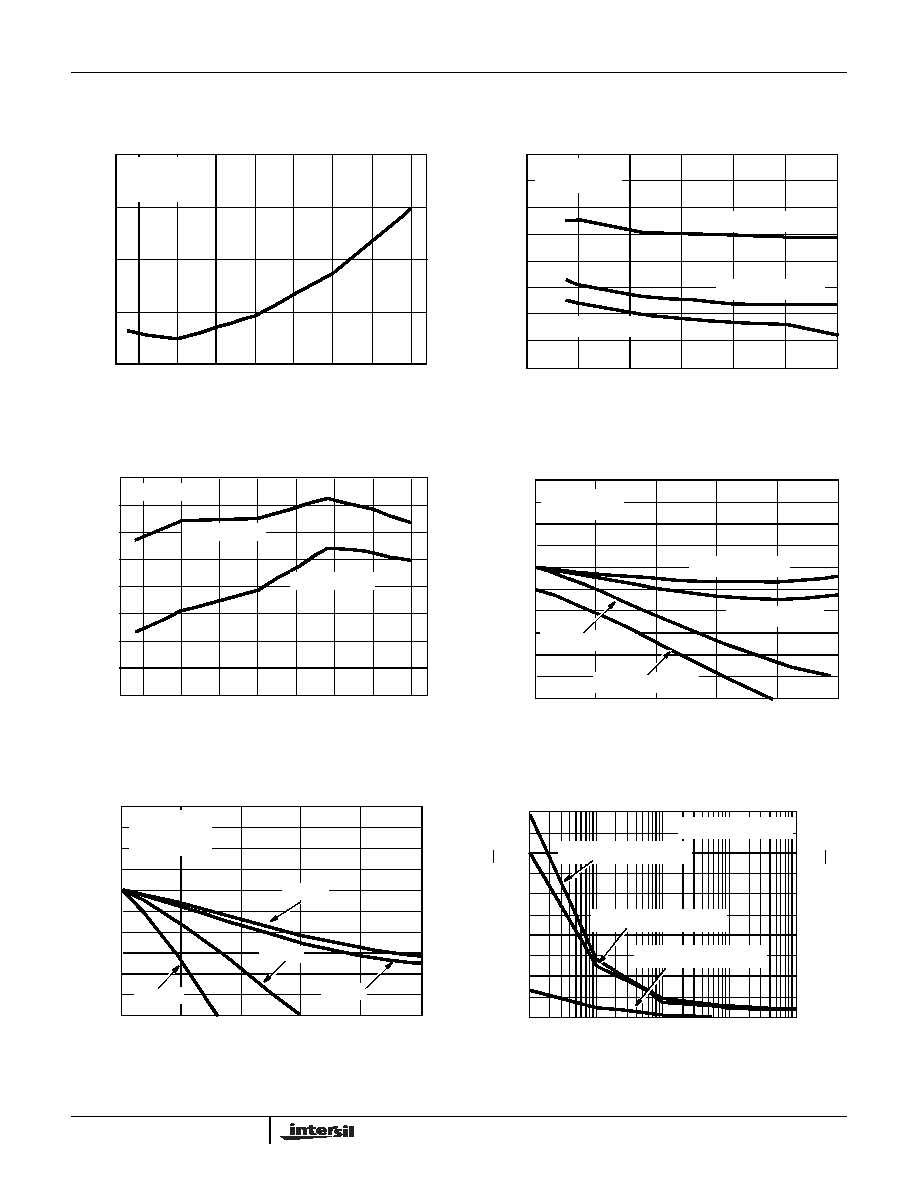
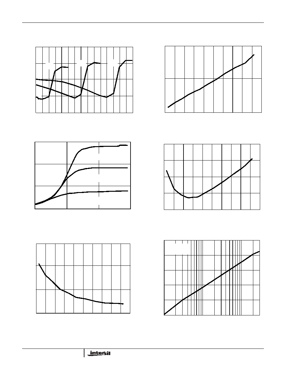
FIGURE 20. PROPAGATION DELAY vs TEMPERATURE
FIGURE 21. PROPAGATION DELAY vs SUPPLY VOLTAGE
FIGURE 22. FIGURE 22. SLEW RATE vs TEMPERATURE
FIGURE 23. NON-INVERTING GAIN FLATNESS vs FREQUENCY
FIGURE 24. INVERTING GAIN FLATNESS vs FREQUENCY
FIGURE 25. INPUT NOISE CHARACTERISTICS
Typical Performance Curves
V
SUPPLY
=
±
5V, A
V
= +1, R
F
= 1k
,
R
L
= 400
,
T
A
= 25
o
C,
Unless Otherwise Specified (Continued)
TEMPERATURE (C)
-50
-25
0
25
50
75
100
125
8.0
7.5
7.0
6.5
6.0
P
R
O
P
AG
AT
IO
N DE
L
A
Y
(
n
s
)
R
L
= 100
V
OUT
= 1.0V
P-P
A
V
= +1
SUPPLY VOLTAGE (
±
V)
P
R
O
P
AG
AT
IO
N D
E
L
A
Y
(
n
s
)
12
10
8
6
4
3
5
7
9
11
13
15
R
LOAD
= 100
V
OUT
= 1.0V
P-P
A
V
= +10, R
F
= 383
A
V
= +2, R
F
= 681
A
V
= +1, R
F
= 1k
TEMPERATURE (
o
C)
-50
-25
0
25
50
75
100
125
500
450
400
350
300
250
200
150
100
S
L
EW
R
A
T
E (
V
/
µ
s)
V
OUT
= 2V
P-P
+ SLEW RATE
- SLEW RATE
A
V
= +1, R
F
= 1k
FREQUENCY (MHz)
5
10
15
20
25
30
0.8
0.6
0.4
0.2
0
-0.2
-0.4
-0.6
-0.8
-1.0
-1.2
NO
RM
AL
IZ
E
D
G
A
I
N
(
d
B)
V
OUT
= 0.2V
P-P
C
L
= 10pF
A
V
= +2, R
F
= 681
A
V
= +5, R
F
= 1k
A
V
= +10, R
F
= 383
0.8
0.6
0.4
0.2
0
-0.2
-0.4
-0.6
-0.8
-1.0
-1.2
NO
RM
AL
IZ
E
D
G
A
IN
(
d
B)
FREQUENCY (MHz)
5
10
15
20
25
30
V
OUT
= 0.2V
P-P
C
L
= 10pF
A
V
= -1
A
V
= -2
A
V
= -5
A
V
= -10
R
F
= 750
FREQUENCY (kHz)
0.01
0.1
1
10
100
VO
L
T
A
G
E
N
O
I
S
E (
n
V/
Hz
)
CURRE
NT
NO
IS
E
(
p
A/
Hz
)
100
80
60
40
20
0
1000
800
600
400
200
0
A
V
= +10, R
F
= 383
-INPUT NOISE CURRENT
+INPUT NOISE CURRENT
INPUT NOISE VOLTAGE
HA5023
11
FIGURE 26. INPUT OFFSET VOLTAGE vs TEMPERATURE
FIGURE 27. +INPUT BIAS CURRENT vs TEMPERATURE
FIGURE 28. -INPUT BIAS CURRENT vs TEMPERATURE
FIGURE 29. TRANSIMPEDANCE vs TEMPERATURE
FIGURE 30. SUPPLY CURRENT vs SUPPLY VOLTAGE
FIGURE 31. REJECTION RATIO vs TEMPERATURE
Typical Performance Curves
V
SUPPLY
=
±
5V, A
V
= +1, R
F
= 1k
,
R
L
= 400
,
T
A
= 25
o
C,
Unless Otherwise Specified (Continued)
1.5
1.0
0.5
0.0
-60
-40
-20
0
40
60
80
100
120
140
20
V
IO
(m
V
)
TEMPERATURE (
o
C)
2
0
-2
-4
-60
-40
-20
0
40
60
80
100
120 140
20
BIAS
CURRE
NT
(
µ
A)
TEMPERATURE (
o
C)
22
20
18
16
-60
-40
-20
0
40
60
80
100
120 140
20
TEMPERATURE (
o
C)
BIAS
CUR
RE
NT
(
µ
A)
TEMPERATURE (
o
C)
4000
3000
2000
1000
T
RANS
I
M
P
E
DANCE
(
k
)
-60
-40
-20
0
40
60
80
100
120
140
20
3
4
5
6
7
8
9
10
11
12
13
14
15
25
20
15
10
5
I
CC
(m
A
)
SUPPLY VOLTAGE (
±
V)
125
o
C
55
o
C
25
o
C
58
60
62
64
66
68
70
72
74
-100
-50
0
50
100
150
+PSRR
-PSRR
CMRR
200
250
TEMPERATURE (
o
C)
RE
J
E
CT
IO
N R
A
T
I
O
(
d
B)
HA5023
12
FIGURE 32. SUPPLY CURRENT vs DISABLE INPUT VOLTAGE
FIGURE 33. OUTPUT SWING vs TEMPERATURE
FIGURE 34. OUTPUT SWING vs LOAD RESISTANCE
FIGURE 35. INPUT OFFSET VOLTAGE CHANGE BETWEEN
CHANNELS vs TEMPERATURE
FIGURE 36. INPUT BIAS CURRENT CHANGE BETWEEN
CHANNELS vs TEMPERATURE
FIGURE 37. CHANNEL SEPARATION vs FREQUENCY
Typical Performance Curves
V
SUPPLY
=
±
5V, A
V
= +1, R
F
= 1k
,
R
L
= 400
,
T
A
= 25
o
C,
Unless Otherwise Specified (Continued)
1
0
2
3
4
5
6
7
8
9 10 11 12 13 14 15
DISABLE INPUT VOLTAGE (V)
40
30
20
10
0
S
U
P
P
L
Y
CURRE
NT
(
m
A)
+5V
+10V
+15V
4.0
3.8
3.6
-60
-40
-20
0
40
60
80
100 120 140
20
TEMPERATURE (
o
C)
O
U
T
P
UT
S
W
ING
(
V
)
0.01
0.10
1.00
10.00
30
20
10
0
V
OU
T
(V
P-
P
)
LOAD RESISTANCE (k
)
V
CC
=
±
15V
V
CC
=
±
10V
V
CC
=
±
4.5V
-60
-40
-20
0
40
60
80
100
120
140
20
1.2
1.1
1.0
0.9
0.8
V
IO
(mV
)
TEMPERATURE (
o
C)
-60
-40
-20
1.5
1.0
0.5
0.0
TEMPERATURE (
o
C)
BIAS
CURRE
NT
(
µ
A)
40
60
80
100
120
140
20
0
-30
-40
-50
-60
-70
-80
0.1
1
10
30
S
E
P
ARAT
IO
N (
d
B)
FREQUENCY (MHz)
A
V
= +1
V
OUT
= 2V
P-P
HA5023

13
FIGURE 38. DISABLE FEEDTHROUGH vs FREQUENCY
FIGURE 39. TRANSIMPEDANCE vs FREQUENCY
FIGURE 40. TRANSIMPEDENCE vs FREQUENCY
Typical Performance Curves
V
SUPPLY
=
±
5V, A
V
= +1, R
F
= 1k
,
R
L
= 400
,
T
A
= 25
o
C,
Unless Otherwise Specified (Continued)
-20
-40
-50
-60
-70
-80
0.1
1
10
20
F
E
E
D
T
HRO
UG
H (
d
B)
FREQUENCY (MHz)
-30
-10
0
DISABLE = 0V
V
IN
= 5V
P-P
R
F
= 750
-135
-90
-45
0
45
90
135
180
10
1
0.1
0.01
0.001
0.001
0.01
0.1
1
10
100
PH
A
SE A
N
G
L
E (
D
E
G
R
E
ES
)
T
RANS
IM
P
E
DANCE
(
M
)
R
L
= 100
FREQUENCY (MHz)
-135
-90
-45
0
45
90
135
180
10
1
0.1
0.01
0.001
0.001
0.01
0.1
1
10
100
P
HAS
E
ANG
L
E
(
D
E
G
RE
E
S
)
R
L
= 400
FREQUENCY (MHz)
T
RANS
IM
P
E
DANC
E
(
M
)
HA5023
14
All Intersil U.S. products are manufactured, assembled and tested utilizing ISO9000 quality systems.
Intersil Corporation's quality certifications can be viewed at www.intersil.com/design/quality
Intersil products are sold by description only. Intersil Corporation reserves the right to make changes in circuit design, software and/or specifications at any time without
notice. Accordingly, the reader is cautioned to verify that data sheets are current before placing orders. Information furnished by Intersil is believed to be accurate and
reliable. However, no responsibility is assumed by Intersil or its subsidiaries for its use; nor for any infringements of patents or other rights of third parties which may result
from its use. No license is granted by implication or otherwise under any patent or patent rights of Intersil or its subsidiaries.
For information regarding Intersil Corporation and its products, see www.intersil.com
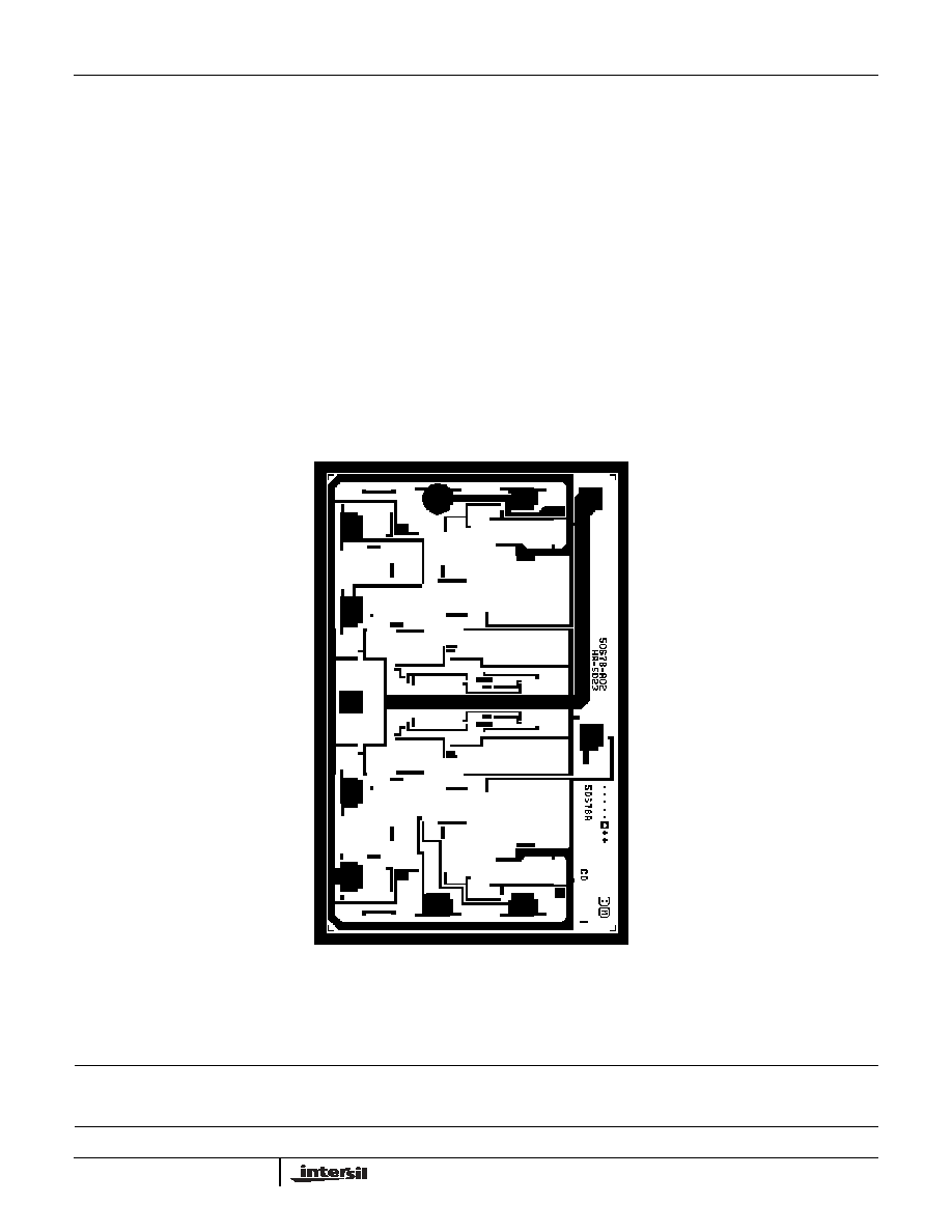
Die Characteristics
DIE DIMENSIONS:
1650
µ
m x 2540
µ
m x 483
µ
m
METALLIZATION:
Type: Metal 1: AlCu (1%)
Thickness: Metal 1: 8k
≈
±
0.4k
≈
Type: Metal 2: AlCu (1%)
Thickness: Metal 2: 16k
≈
±
0.8k
≈
SUBSTRATE POTENTIAL (Powered Up):
V-
PASSIVATION:
Type: Nitride
Thickness: 4k
≈
±
0.4k
≈
TRANSISTOR COUNT:
124
PROCESS:
High Frequency Bipolar Dielectric Isolation
Metallization Mask Layout
HA5023
V+
NC
V-
NC
NC
-IN
+IN
-IN1
OUT2
+IN1
OUT
HA5023