 | –≠–ª–µ–∫—Ç—Ä–æ–Ω–Ω—ã–π –∫–æ–º–ø–æ–Ω–µ–Ω—Ç: HA-5147 | –°–∫–∞—á–∞—Ç—å:  PDF PDF  ZIP ZIP |
1
TM
File Number
2910.6
CAUTION: These devices are sensitive to electrostatic discharge; follow proper IC Handling Procedures.
1-888-INTERSIL or 321-724-7143
|
Intersil and Design is a trademark of Intersil Corporation.
|
Copyright
©
Intersil Corporation 2000
HA-5147
120MHz, Ultra-Low Noise Precision
Operational Amplifiers
The HA-5147 operational amplifier features an unparalleled
combination of precision DC and wideband high speed
characteristics. Utilizing the Intersil D. I. technology and
advanced processing techniques, this unique design unites
low noise (3.2nV/
Hz) precision instrumentation
performance with high speed (35V/
µ
s) wideband capability.
This amplifier's impressive list of features include low V
OS
(30mV), wide gain bandwidth (120MHz), high open loop gain
(1500V/mV), and high CMRR (120dB). Additionally, this
flexible device operates over a wide supply range (
±
5V to
±
20V) while consuming only 140mW of power.
Using the HA-5147 allows designers to minimize errors while
maximizing speed and bandwidth in applications requiring
gains greater than ten.
This device is ideally suited for low level transducer signal
amplifier circuits. Other applications which can utilize the
HA-5147's qualities include instrumentation amplifiers, pulse
or RF amplifiers, audio preamplifiers, and signal conditioning
circuits.
This device can easily be used as a design enhancement by
directly replacing the 725, OP25, OP06, OP07, OP27 and
OP37 where gains are greater than ten. For military grade
product, refer to the HA-5147/883 data sheet.
Features
∑ Slew Rate . . . . . . . . . . . . . . . . . . . . . . . . . . . . . . . . 35V/
µ
s
∑ Wide Gain Bandwidth (A
V
10) . . . . . . . . . . . . . . 120MHz
∑ Low Noise. . . . . . . . . . . . . . . . . . . . . . 3.2nV/
Hz at 1kHz
∑ Low V
OS
. . . . . . . . . . . . . . . . . . . . . . . . . . . . . . . . . . 30
µ
V
∑ High CMRR . . . . . . . . . . . . . . . . . . . . . . . . . . . . . . 120dB
∑ High Gain . . . . . . . . . . . . . . . . . . . . . . . . . . . . . 1500V/mV
Applications
∑ High Speed Signal Conditioners
∑ Wide Bandwidth Instrumentation Amplifiers
∑ Low Level Transducer Amplifiers
∑ Fast, Low Level Voltage Comparators
∑ Highest Quality Audio Preamplifiers
∑ Pulse/RF Amplifiers
∑ For Further Design Ideas See Application Note AN553
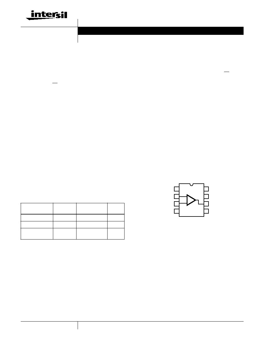
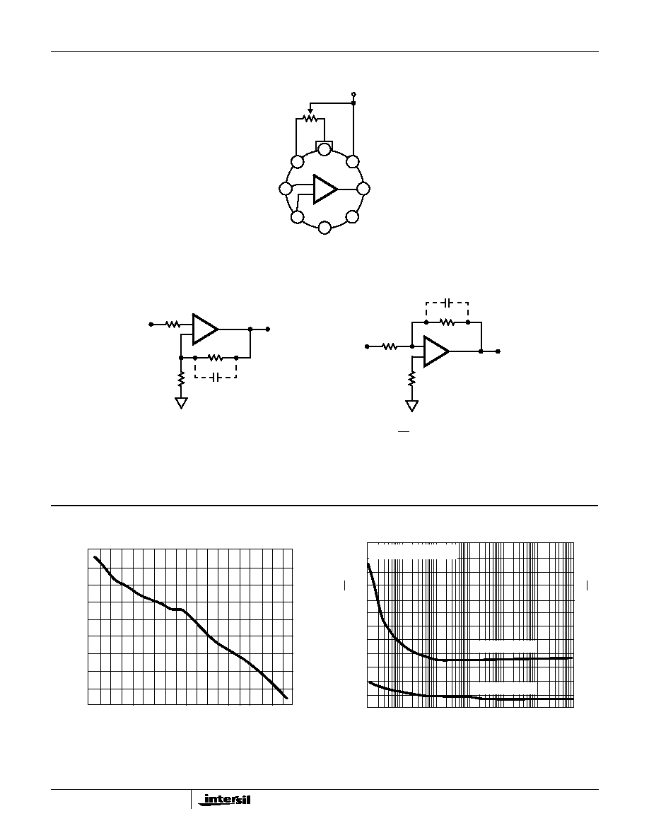
Pinout
HA-5147 (CERDIP, SOIC)
TOP VIEW
Ordering Information
PART NUMBER
(BRAND)
TEMP.
RANGE (
o
C)
PACKAGE
PKG.
NO.
HA7-5147-2
-55 to 125
8 Ld CERDIP
F8.3A
HA7-5147-5
0 to 75
8 Ld CERDIP
F8.3A
HA9P5147-9
(H51479)
-40 to 85
8 Ld SOIC
M8.15
1
2
3
4
8
7
6
5
BAL
V+
OUT
NC
BAL
-IN
+IN
V-
+
-
Data Sheet
April 2000
[ /Title
(HA-
5147)
/Sub-
ject
(120M
Hz,
Ultra-
Low
Noise
Preci-
sion
Opera-
tional
Ampli-
fiers)
/Autho
r ()
/Key-
words
(Inter-
sil
Corpo-
ration,
Semi-
con-
ductor,
single,
opera-
tional
ampli-
fier,
low
power
op
amp,
low
input
bias
2
Absolute Maximum Ratings
T
A
= 25
o
C
Thermal Information
Voltage Between V+ and V- Terminals. . . . . . . . . . . . . . . . . . . . 44V
Differential Input Voltage (Note 1) . . . . . . . . . . . . . . . . . . . . . . . 0.7V
Output Current . . . . . . . . . . . . . . . . . . . Full Short Circuit Protection
Operating Conditions
Temperature Range
HA-5147-2 . . . . . . . . . . . . . . . . . . . . . . . . . . . . . . -55
o
C to 125
o
C
HA-5147-5 . . . . . . . . . . . . . . . . . . . . . . . . . . . . . . . . 0
o
C to 75
o
C
HA-5147-9 . . . . . . . . . . . . . . . . . . . . . . . . . . . . . . . -40
o
C to 85
o
C
Thermal Resistance (Typical, Note 2)
JA
(
o
C/W)
JC
(
o
C/W)
CERDIP Package . . . . . . . . . . . . . . . . .
135
50
SOIC Package . . . . . . . . . . . . . . . . . . .
158
N/A
Maximum Junction Temperature (Hermetic Package) . . . . . . . .175
o
C
Maximum Junction Temperature (Plastic Package) . . . . . . . . . .150
o
C
Maximum Storage Temperature Range . . . . . . . . . . -65
o
C to 150
o
C
Maximum Lead Temperature (Soldering 10s) . . . . . . . . . . . . 300
o
C
(SOIC - Lead Tips Only)
CAUTION: Stresses above those listed in "Absolute Maximum Ratings" may cause permanent damage to the device. This is a stress only rating and operation of the
device at these or any other conditions above those indicated in the operational sections of this specification is not implied.
NOTES:
1. For differential input voltages greater than 0.7V, the input current must be limited to 25mA to protect the back-to-back input diodes.
2.
JA
is measured with the component mounted on an evaluation PC board in free air.
Electrical Specifications
V
SUPPLY
=
±
15V, C
L
50pF, R
S
100
PARAMETER
TEST CONDITIONS
TEMP.
(
o
C)
MIN
TYP
MAX
UNITS
INPUT CHARACTERISTICS
Offset Voltage
25
-
30
100
µ
V
Full
-
70
300
µ
V
Average Offset Voltage Drift
Full
-
0.4
1.8
µ
V/
o
C
Bias Current
25
-
15
80
nA
Full
-
35
150
nA
Offset Current
25
-
12
75
nA
Full
-
30
135
nA
Common Mode Range
Full
±
10.3
±
11.5
-
V
Differential Input Resistance (Note 3)
25
0.8
4
-
M
Input Noise Voltage (Note 4)
0.1Hz to 10Hz
25
-
0.09
0.25
µ
V
P-P
Input Noise Voltage Density (Note 5)
f = 10Hz
25
-
3.8
8.0
nV/
Hz
f = 100Hz
-
3.3
4.5
nV/
Hz
f = 1000Hz
-
3.2
3.8
nV/
Hz
Input Noise Current Density (Note 5)
f = 10Hz
25
-
1.7
-
pA/
Hz
f = 100Hz
-
1.0
-
pA/
Hz
f = 1000Hz
-
0.4
0.6
pA/
Hz
TRANSFER CHARACTERISTICS
Minimum Stable Gain
25
10
-
-
V/V
Large Signal Voltage Gain
V
OUT
=
±
10V, R
L
= 2k
25
700
1500
-
V/mV
Full
300
800
-
V/mV
HA-5147
3
Common Mode Rejection Ratio
V
CM
=
±
10V
Full
100
120
-
dB
Gain-Bandwidth-Product
f = 10kHz
25
120
140
-
MHz
f = 1MHz
-
120
-
MHz
OUTPUT CHARACTERISTICS
Output Voltage Swing
R
L
= 600
25
±
10.0
±
11.5
-
V
R
L
= 2k
Full
±
11.4
±
13.5
-
V
Full Power Bandwidth (Note 6)
25
445
500
-
kHz
Output Resistance
Open Loop
25
-
70
-
Output Current
25
16.5
25
-
mA
TRANSIENT RESPONSE (Note 7)
Rise Time
25
-
22
50
ns
Slew Rate
V
OUT
=
±
3V
25
28
35
-
V/
µ
s
Settling Time
Note 8
25
-
400
-
ns
Overshoot
25
-
20
40
%
POWER SUPPLY CHARACTERISTICS
Supply Current
25
-
3.5
-
mA
Full
-
-
4.0
mA
Power Supply Rejection Ratio
V
S
=
±
4V to
±
18V
Full
-
16
51
µ
V/V
NOTES:
3. This parameter value is based upon design calculations.
4. Refer to Typical Performance section of the data sheet.
5. The limits for this parameter are guaranteed based on lab characterization, and reflect lot-to-lot variation.
6. Full power bandwidth guaranteed based on slew rate measurement using:
.
7. Refer to Test Circuits section of the data sheet.
8. Settling time is specified to 0.1% of final value for a 10V output step and A
V
= -10.
Electrical Specifications
V
SUPPLY
=
±
15V, C
L
50pF, R
S
100
(Continued)
PARAMETER
TEST CONDITIONS
TEMP.
(
o
C)
MIN
TYP
MAX
UNITS
FPBW
Slew Rate
2
V
PEAK
-----------------------------
=
HA-5147
4
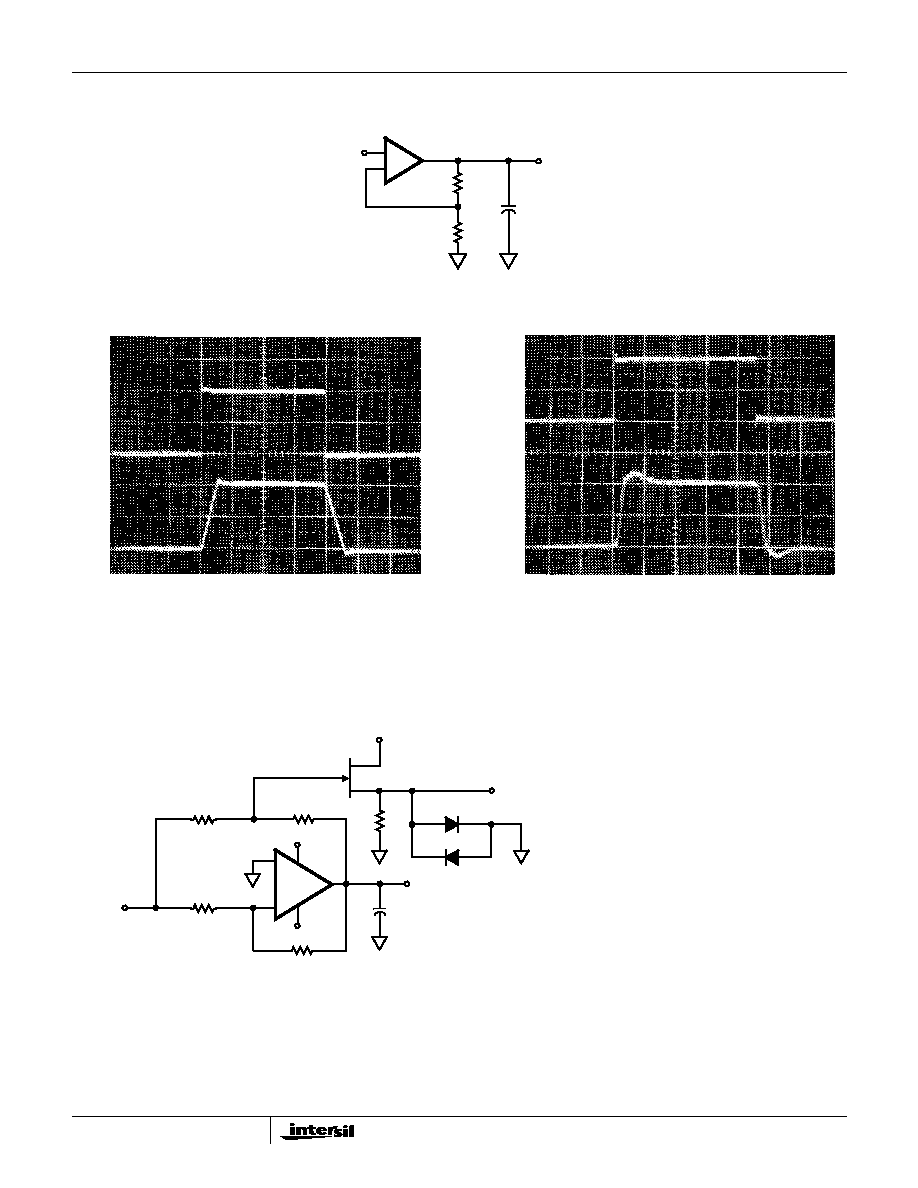
Test Circuits and Waveforms
FIGURE 1. LARGE AND SMALL SIGNAL RESPONSE TEST CIRCUIT
Vertical Scale: Input = 0.5V/Div.
Output = 5V/Div.
Horizontal Scale: 500ns/Div.
LARGE SIGNAL RESPONSE
Vertical Scale: Input = 10mV/Div.
Output = 100mV/Div.
Horizontal Scale: 100ns/Div.
SMALL SIGNAL RESPONSE
FIGURE 2. SETTLING TIME TEST CIRCUIT
+
IN
OUT
50pF
1.8k
200
-
OUT
IN
OUT
IN
NOTES:
9. A
V
= -10.
10. Feedback and summing resistors should be 0.1%
matched.
11. Clipping diodes are optional. HP5082-2810 recommended.
+
-15V
+15V
50pF
2N4416
5k
+15V
2k
200
2k
TO
OSCILLOSCOPE
500
V
OUT
V
IN
AUT
-
HA-5147
5
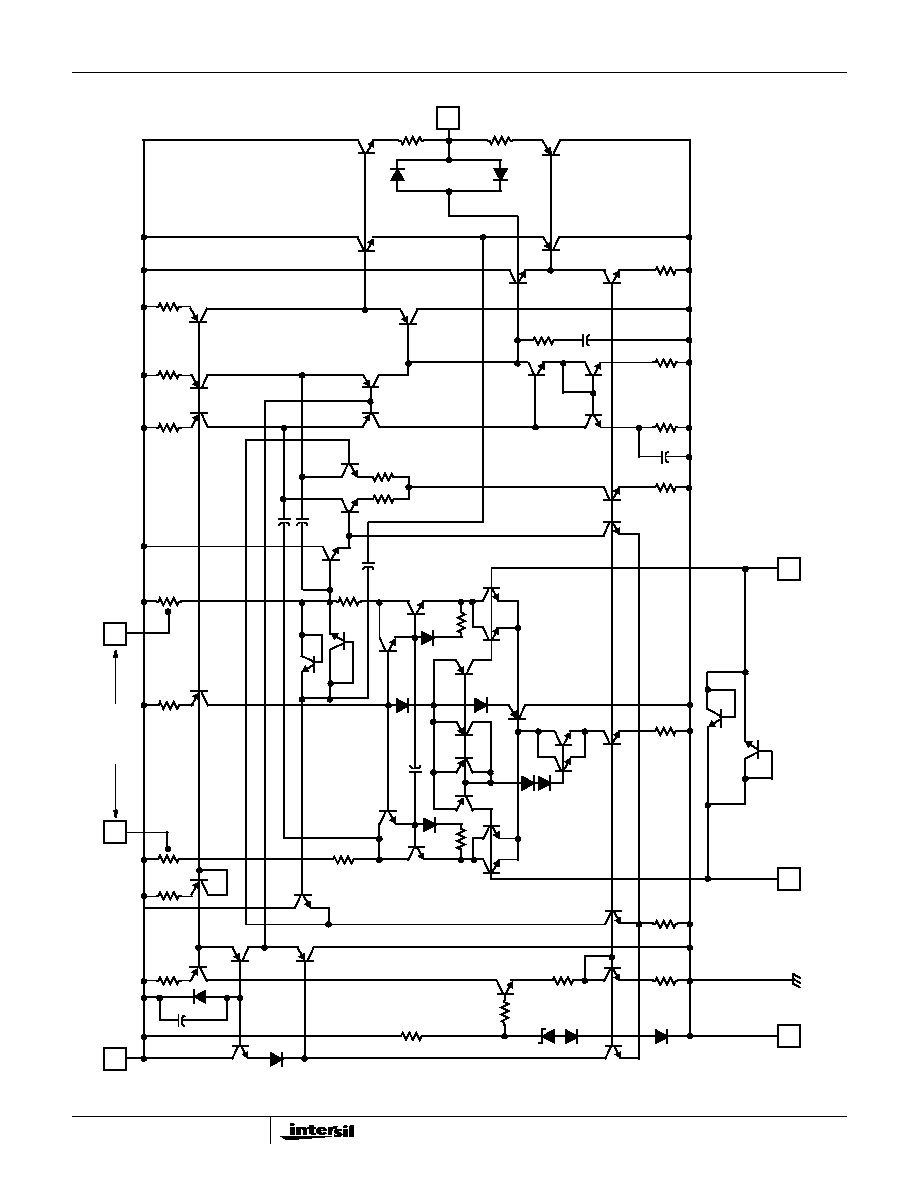
Schematic Diagram
4
3
2
D
60
R
5
R
6
Q
N24
Q
N25
D
59
Z
58
R
24
Q
N12
R
4
R
14
D
8
Q
N45
C
7
D
1
R
15
Q
P37
Q
P55
Q
P56
Q
N19
R
1A
7
R
25
R
1
Q
P32
1
8
BALANCE
R
16
Q
P35
Q
N46
Q
N47
R
2A
C
1
Q
N13
C
4
C
5
R
2
Q
N51
Q
N3
D
53
R
9
Q
N2
Q
P
27
Q
N2A
C
6
Q
P36A
Q
P36
D
9
Q
N52
Q
N4
D
54
Q
P26
R
18
Q
N1A
Q
N1
Q
P40
D
41
D
22
D
23
Q
N42A
Q
N42
Q
N39
R
8
Q
N10
Q
N11
Q
N48
Q
N49
R
10
C
3
Q
N5
C
2
R
22
Q
N14
Q
N15
R
7
R
3
R
20
Q
P43
R
21
Q
P44
R
17
Q
P26
Q
P17
Q
P16
Q
N7
Q
N6
Q
N29
Q
N18
Q
P30
D
33
D
34
Q
N20
R
12
OUT-
R
13
Q
P21
6
PUT
R
23
Q
N50
R
11
Q
N57
Q
P38
R
19
HA-5147
6
Application Information
FIGURE 3.
SUGGESTED OFFSET VOLTAGE ADJUSTMENT
NOTE:
Low resistances are preferred for low noise applications as a 1k
resistor has 4nV/
Hz of thermal noise. Total resistances of greater than
10k
on either input can reduce stability. In most high resistance applications, a few picofarads of capacitance across the feedback resistor will im-
prove stability.
FIGURE 4. SUGGESTED STABILITY CIRCUITS
2
4
6
1
3
7
5
8
+
V+
10K
R
P
-
NOTE: Tested Offset Adjustment
Range is |V
OS
+1mV| minimum re-
ferred to output. Typical range is
±
4mV
with R
P
= 10k
.
+
R
1
C
S
R
3
R
2
+
R
1
R
2
R
3
C
S
-
-
Typical Performance Curves
T
A
= 25
o
C, V
SUPPLY
=
±
15V, Unless Otherwise Specified
FIGURE 5. TYPICAL OFFSET VOLTAGE vs TEMPERATURE
FIGURE 6. NOISE CHARACTERISTICS
TEMPERATURE (
o
C)
OFFSET VOLTAGE (
µ
V)
-60
-40
-20
0
20
40
60
80
120
100
-60
-50
-40
-30
-20
-10
0
10
30
20
V
S
=
±
15V, T
A
= 25
o
C
NOISE VOLTAGE
NOISE CURRENT
1M
100K
10K
1K
100
10
1
FREQUENCY (Hz)
0
2
4
6
8
10
12
VOLTAGE NOISE (nV/
Hz)
CURRENT NOISE (pA/
Hz)
0
1
2
3
4
5
6
HA-5147
7
FIGURE 7. NOISE vs SUPPLY VOLTAGE
FIGURE 8. CMRR vs FREQUENCY
FIGURE 9. PSRR vs FREQUENCY
FIGURE 10. OPEN LOOP GAIN AND PHASE vs FREQUENCY
FIGURE 11. A
VOL
AND V
OUT
vs LOAD RESISTANCE
FIGURE 12. NORMALIZED SLEW RATE vs TEMPERATURE
Typical Performance Curves
T
A
= 25
o
C, V
SUPPLY
=
±
15V, Unless Otherwise Specified (Continued)
T
A
= 25
o
C
SUPPLY VOLTAGE (
±
V)
4
6
8
10
12
14
16
20
18
0.14
0.12
0.1
0.08
0.06
0.04
0.02
0
INPUT NOISE V
O
L
T
A
GE (
µ
V
P-P
)
FREQUENCY (Hz)
CMRR (dB)
10
100
1K
10K
100K
1M
10M
0
40
80
120
160
V
S
=
±
15V
T
A
= 25
o
C
FREQUENCY (Hz)
PSRR (dB)
10
100
1K
10K
100K
1M
100
80
60
20
120
40
0
T
A
= 25
o
C
FREQUENCY (Hz)
GAIN (dB)
100
1K
10K
100K
1M
10M
0
40
60
100
120
100M
180
90
0
80
20
PHASE (DEGREES)
GAIN
PHASE
T
A
= 25
o
C
LOAD RESISTANCE (k
)
0
4
6
8
10
17
16
15
13
12
10
7
4
A
VO
L
(100kV/V) AND V
OUT
(V)
2
14
11
9
8
6
5
A
VOL
V
OUT
TEMPERATURE (
o
C)
-60
-40
-20
0
20
40
60
80
120
100
0.95
0.96
0.97
0.98
0.99
1.0
1.01
1.02
1.03
1.04
1.05
SLEW RA
TE NORMALIZED T
O
1 A
T
30
o
C
R
L
= 2K, C
L
= 50pF, T
A
= 25
o
C
HA-5147
8
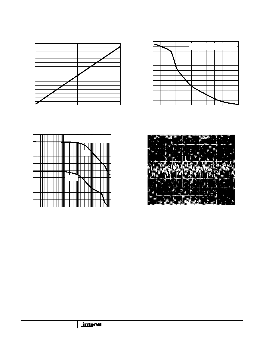
FIGURE 13. SUPPLY CURRENT vs TEMPERATURE
FIGURE 14. V
OUT
MAX (UNDISTORTED SINEWAVE OUTPUT)
vs FREQUENCY
FIGURE 15. CLOSED LOOP GAIN AND PHASE vs FREQUENCY
FIGURE 16. PEAK-TO-PEAK NOISE VOLTAGE (0.1Hz TO 10Hz)
Typical Performance Curves
T
A
= 25
o
C, V
SUPPLY
=
±
15V, Unless Otherwise Specified (Continued)
TEMPERATURE (
o
C)
-55
25
125
2.82
SUPPL
Y CURRENT (mA)
V
O
= 0V, V
S
=
±
15V
2.80
2.78
2.76
2.74
2.72
2.70
2.68
FREQUENCY (MHz)
OUTPUT V
O
L
T
A
GE (V
P-P
)
0
0.4
0.8
1.2
1.6
2
4
16
20
24
28
12
8
R
L
= 2K, C
L
= 50pF, T
A
= 25
o
C
FREQUENCY (Hz)
GAIN (dB)
1K
10K
100K
1M
10M
0
20
30
100M
180
90
0
40
10
PHASE (DEGREES)
GAIN
PHASE
R
L
= 2K, C
L
= 50pF, T
A
= 25
o
C
A
CL
= 25,000V/V; E
N
= 0.08
µ
V
P-P
RTI
Horizontal Scale = 1s/Div.; Vertical Scale = 0.002
µ
V/Div.
HA-5147
9
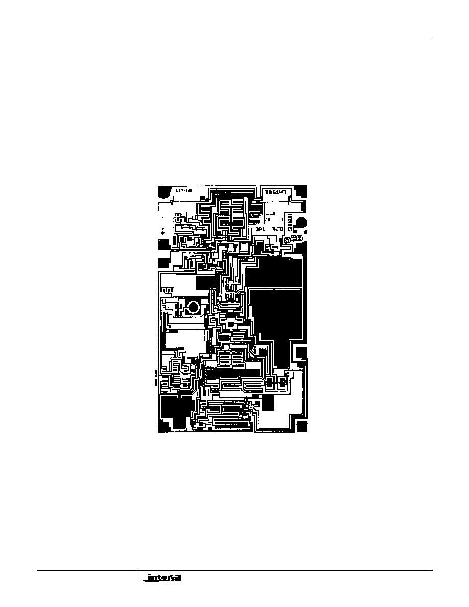
Die Characteristics
DIE DIMENSIONS:
104 mils x 65 mils x 19 mils
2650
µ
m x 1650
µ
m x 483
µ
m
METALLIZATION:
Type: Al, 1% Cu
Thickness: 16k
≈
±
2k
≈
SUBSTRATE POTENTIAL (POWERED UP):
V-
PASSIVATION:
Type: Nitride (Si
3
N
4
) over Silox (SiO
2
, 5% Phos.)
Silox Thickness: 12k
≈
±
2k
≈
Nitride Thickness: 3.5k
≈
±
1.5k
≈
TRANSISTOR COUNT:
63
PROCESS:
Bipolar Dielectric Isolation
Metallization Mask Layout
HA-5147
BAL
BAL
V+
OUT
NC
V-
+IN
-IN
HA-5147
10
HA-5147
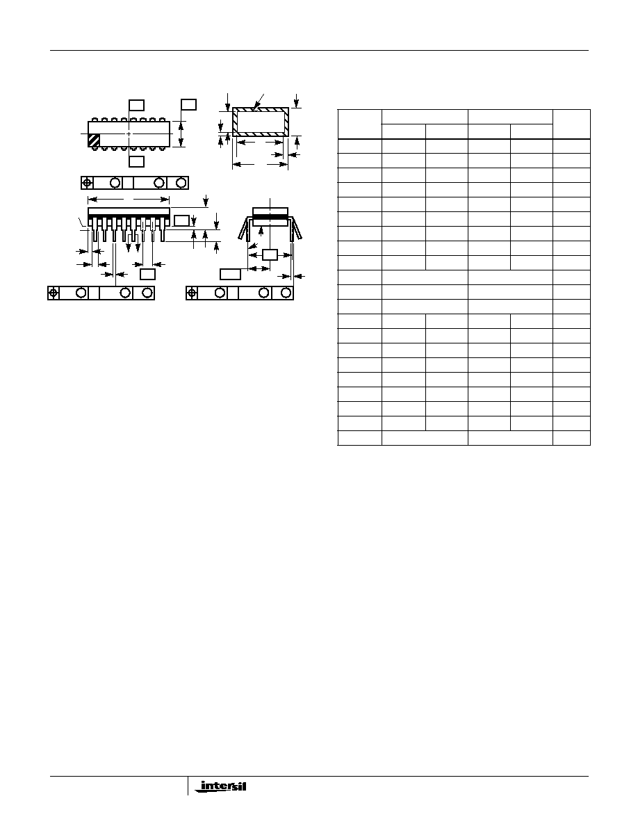
Ceramic Dual-In-Line Frit Seal Packages (CERDIP)
NOTES:
1. Index area: A notch or a pin one identification mark shall be locat-
ed adjacent to pin one and shall be located within the shaded
area shown. The manufacturer's identification shall not be used
as a pin one identification mark.
2. The maximum limits of lead dimensions b and c or M shall be
measured at the centroid of the finished lead surfaces, when
solder dip or tin plate lead finish is applied.
3. Dimensions b1 and c1 apply to lead base metal only. Dimension
M applies to lead plating and finish thickness.
4. Corner leads (1, N, N/2, and N/2+1) may be configured with a
partial lead paddle. For this configuration dimension b3 replaces
dimension b2.
5. This dimension allows for off-center lid, meniscus, and glass
overrun.
6. Dimension Q shall be measured from the seating plane to the
base plane.
7. Measure dimension S1 at all four corners.
8. N is the maximum number of terminal positions.
9. Dimensioning and tolerancing per ANSI Y14.5M - 1982.
10. Controlling dimension: INCH
bbb
C A - B
S
c
Q
L
A
SEATING
BASE
D
PLANE
PLANE
-D-
-A-
-C-
-B-
D
E
S1
b2
b
A
e
M
c1
b1
(c)
(b)
SECTION A-A
BASE
LEAD FINISH
METAL
e
A/2
A
M
S
S
ccc
C A - B
M
D
S
S
aaa
C A - B
M
D
S
S
e
A
F8.3A
MIL-STD-1835 GDIP1-T8 (D-4, CONFIGURATION A)
8 LEAD CERAMIC DUAL-IN-LINE FRIT SEAL PACKAGE
SYMBOL
INCHES
MILLIMETERS
NOTES
MIN
MAX
MIN
MAX
A
-
0.200
-
5.08
-
b
0.014
0.026
0.36
0.66
2
b1
0.014
0.023
0.36
0.58
3
b2
0.045
0.065
1.14
1.65
-
b3
0.023
0.045
0.58
1.14
4
c
0.008
0.018
0.20
0.46
2
c1
0.008
0.015
0.20
0.38
3
D
-
0.405
-
10.29
5
E
0.220
0.310
5.59
7.87
5
e
0.100 BSC
2.54 BSC
-
eA
0.300 BSC
7.62 BSC
-
eA/2
0.150 BSC
3.81 BSC
-
L
0.125
0.200
3.18
5.08
-
Q
0.015
0.060
0.38
1.52
6
S1
0.005
-
0.13
-
7
90
o
105
o
90
o
105
o
-
aaa
-
0.015
-
0.38
-
bbb
-
0.030
-
0.76
-
ccc
-
0.010
-
0.25
-
M
-
0.0015
-
0.038
2, 3
N
8
8
8
Rev. 0 4/94
11
All Intersil semiconductor products are manufactured, assembled and tested under ISO9000 quality systems certification.
Intersil semiconductor products are sold by description only. Intersil Corporation reserves the right to make changes in circuit design and/or specifications at any time with-
out notice. Accordingly, the reader is cautioned to verify that data sheets are current before placing orders. Information furnished by Intersil is believed to be accurate and
reliable. However, no responsibility is assumed by Intersil or its subsidiaries for its use; nor for any infringements of patents or other rights of third parties which may result
from its use. No license is granted by implication or otherwise under any patent or patent rights of Intersil or its subsidiaries.
For information regarding Intersil Corporation and its products, see web site www.intersil.com
Sales Office Headquarters
NORTH AMERICA
Intersil Corporation
P. O. Box 883, Mail Stop 53-204
Melbourne, FL 32902
TEL: (321) 724-7000
FAX: (321) 724-7240
EUROPE
Intersil SA
Mercure Center
100, Rue de la Fusee
1130 Brussels, Belgium
TEL: (32) 2.724.2111
FAX: (32) 2.724.22.05
ASIA
Intersil (Taiwan) Ltd.
7F-6, No. 101 Fu Hsing North Road
Taipei, Taiwan
Republic of China
TEL: (886) 2 2716 9310
FAX: (886) 2 2715 3029
HA-5147
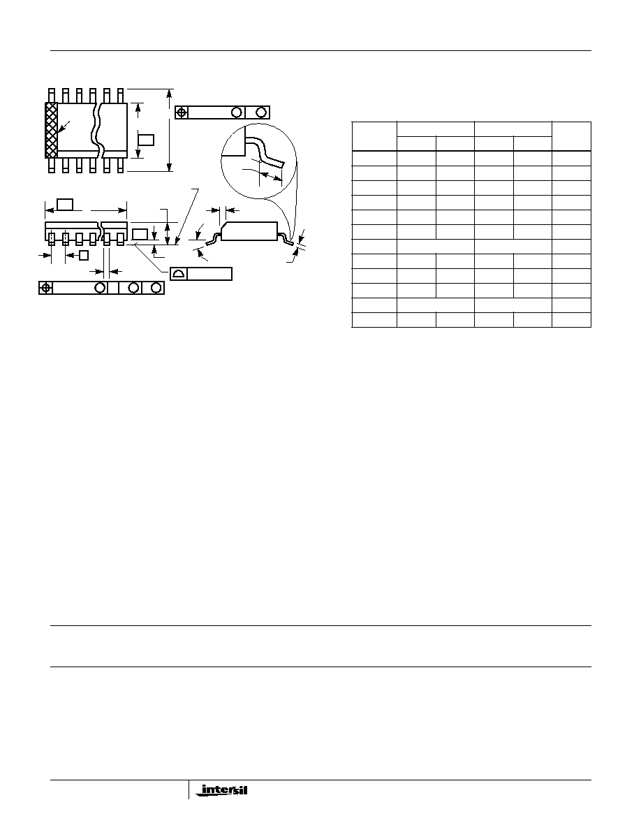
Small Outline Plastic Packages (SOIC)
INDEX
AREA
E
D
N
1
2
3
-B-
0.25(0.010)
C A
M
B S
e
-A-
L
B
M
-C-
A1
A
SEATING PLANE
0.10(0.004)
h x 45
o
C
H
0.25(0.010)
B
M
M
NOTES:
1. Symbols are defined in the "MO Series Symbol List" in Section 2.2 of
Publication Number 95.
2. Dimensioning and tolerancing per ANSI Y14.5M-1982.
3. Dimension "D" does not include mold flash, protrusions or gate burrs.
Mold flash, protrusion and gate burrs shall not exceed 0.15mm (0.006
inch) per side.
4. Dimension "E" does not include interlead flash or protrusions. Inter-
lead flash and protrusions shall not exceed 0.25mm (0.010 inch) per
side.
5. The chamfer on the body is optional. If it is not present, a visual index
feature must be located within the crosshatched area.
6. "L" is the length of terminal for soldering to a substrate.
7. "N" is the number of terminal positions.
8. Terminal numbers are shown for reference only.
9. The lead width "B", as measured 0.36mm (0.014 inch) or greater
above the seating plane, shall not exceed a maximum value of
0.61mm (0.024 inch).
10. Controlling dimension: MILLIMETER. Converted inch dimensions
are not necessarily exact.
M8.15
(JEDEC MS-012-AA ISSUE C)
8 LEAD NARROW BODY SMALL OUTLINE PLASTIC
PACKAGE
SYMBOL
INCHES
MILLIMETERS
NOTES
MIN
MAX
MIN
MAX
A
0.0532
0.0688
1.35
1.75
-
A1
0.0040
0.0098
0.10
0.25
-
B
0.013
0.020
0.33
0.51
9
C
0.0075
0.0098
0.19
0.25
-
D
0.1890
0.1968
4.80
5.00
3
E
0.1497
0.1574
3.80
4.00
4
e
0.050 BSC
1.27 BSC
-
H
0.2284
0.2440
5.80
6.20
-
h
0.0099
0.0196
0.25
0.50
5
L
0.016
0.050
0.40
1.27
6
N
8
8
7
0
o
8
o
0
o
8
o
-
Rev. 0 12/93