 | –≠–ª–µ–∫—Ç—Ä–æ–Ω–Ω—ã–π –∫–æ–º–ø–æ–Ω–µ–Ω—Ç: HCA10014 | –°–∫–∞—á–∞—Ç—å:  PDF PDF  ZIP ZIP |
1
File Number
4769
CAUTION: These devices are sensitive to electrostatic discharge; follow proper IC Handling Procedures.
http://www.intersil.com or 407-727-9207 | Copyright © Intersil Corporation 1999
HCA10014
15MHz, BiMOS Operational Amplifier with
MOSFET Input/CMOS Output
HCA10014 op amp combines the advantage of both CMOS
and bipolar transistors.
Gate protected P-Channel MOSFET (PMOS) transistors are
used in the input circuit to provide very high input
impedance, very low input current, and exceptional speed
performance. The use of PMOS transistors in the input stage
results in common mode input voltage capability down to
0.5V below the negative supply terminal, an important
attribute in single supply applications.
A CMOS transistor pair, capable of swinging the output
voltage to within 10mV of either supply voltage terminal (at
very high values of load impedance), is employed as the
output circuit.
The HCA10014 operates at supply voltages ranging from 5V
to 16V, (
±
2.5V to
±
8V). It can be phase compensated with a
single external capacitor, and have terminals for adjustment
of offset voltage for applications requiring offset null
capability. Terminal provisions are also made to permit
strobing of the output stage.
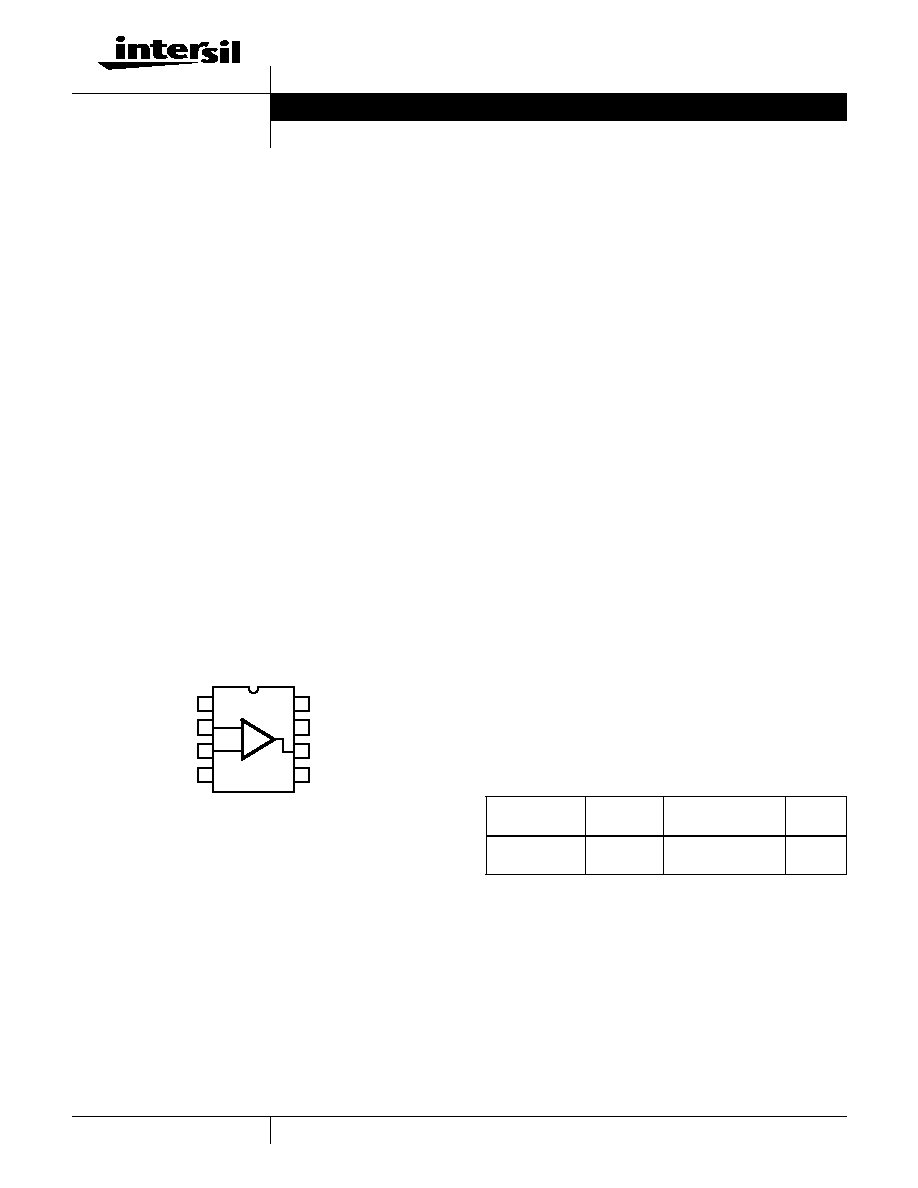
Pinout
HCA10014
(SOIC)
TOP VIEW
Features
∑ MOSFET Input Stage Provides:
- Very High Z
I
= 1.5T
(1.5 x 10
12
) (Typ)
- Very Low I
I
15V Operation. . . . . . . . . . . . . . . . . . . . . . . . . 5pA (Typ)
5V Operation. . . . . . . . . . . . . . . . . . . . . . . . . . 2pA (Typ)
∑ Ideal for Single Supply Applications
∑ Common Mode Input Voltage Range Includes
Negative Supply Rail; Input Terminals can be Swung 0.5V
Below Negative Supply Rail
∑ CMOS Output Stage Permits Signal Swing to Either (or
both) Supply Rails
Applications
∑ Ground Referenced Single Supply Amplifiers
∑ Fast Sample and Hold Amplifiers
∑ Long Duration Timers/Monostables
∑ High Input Impedance Comparators
(Ideal Interface with Digital CMOS)
∑ High Input Impedance Wideband Amplifiers
∑ Voltage Followers (e.g., Follower for Single Supply D/A
Converter)
∑ Voltage Regulators (Permits Control of Output Voltage
Down to 0V)
∑ Peak Detectors
∑ Single Supply Full Wave Precision Rectifiers
∑ Photo Diode Sensor Amplifiers
OFFSET
INV.
NON-INV.
V-
1
2
3
4
8
7
6
5
STROBE
V+
OUTPUT
OFFSET
-
+
NULL
INPUT
INPUT
NULL
Ordering Information
PART NO.
(BRAND)
TEMP.
RANGE (
o
C)
PACKAGE
PKG. NO.
HCA10014
-55 to 125
8 Ld SOIC
Tape and Reel
M8.15
Data Sheet
August 1999
2
Absolute Maximum Ratings
Thermal Information
DC Supply Voltage (Between V+ and V- Terminals) . . . . . . . . . .16V
Differential Input Voltage . . . . . . . . . . . . . . . . . . . . . . . . . . . . . . . .8V
DC Input Voltage . . . . . . . . . . . . . . . . . . . . . . (V+ +8V) to (V- -0.5V)
Input Terminal Current . . . . . . . . . . . . . . . . . . . . . . . . . . . . . . . . 1mA
Output Short Circuit Duration (Note 1). . . . . . . . . . . . . . . . Indefinite
Operating Conditions
Temperature Range . . . . . . . . . . . . . . . . . . . . . . . . . -50
o
C to 125
o
C
Thermal Resistance (Typical, Note 2)
JA
(
o
C/W)
SOIC Package . . . . . . . . . . . . . . . . . . . . . . . . . . . . .
160
Maximum Junction Temperature (Metal Can Package) . . . . . . .175
o
C
Maximum Junction Temperature (Plastic Package) . . . . . . . .150
o
C
Maximum Storage Temperature Range . . . . . . . . . . -65
o
C to 150
o
C
Maximum Lead Temperature (Soldering 10s) . . . . . . . . . . . . .300
o
C
(SOIC - Lead Tips Only)
CAUTION: Stresses above those listed in "Absolute Maximum Ratings" may cause permanent damage to the device. This is a stress only rating and operation of the
device at these or any other conditions above those indicated in the operational sections of this specification is not implied.
NOTES:
1. Short circuit may be applied to ground or to either supply.
2.
JA
is measured with the component mounted on an evaluation PC board in free air.
Electrical Specifications
T
A
= 25
o
C, V+ = 15V, V- = 0V, Unless Otherwise Specified
PARAMETER
SYMBOL
TEST
CONDITIONS
MIN
TYP
MAX
UNITS
Input Offset Voltage
|V
IO
|
V
S
=
±
7.5V
-
8
15
mV
Input Offset Voltage Temperature Drift
V
IO
/
T
-
10
-
µ
V/
o
C
Input Offset Current
|I
IO
|
V
S
=
±
7.5V
-
0.5
30
pA
Input Current
I
I
V
S
=
±
7.5V
-
5
50
pA
Large Signal Voltage Gain
A
OL
V
O
= 10V
P-P
, R
L
= 2k
50
320
-
kV/V
94
110
-
dB
Common Mode Rejection Ratio
CMRR
70
90
-
dB
Common Mode Input Voltage Range
V
ICR
0
-0.5 to 12
10
V
Power Supply Rejection Ratio
V
IO
/
V
S
V
S
=
±
7.5V
-
32
320
µ
V/V
Maximum Output Voltage
V
OM
+
R
L
= 2k
12
13.3
-
V
V
OM
-
R
L
= 2k
-
0.002
0.01
V
V
OM
+
R
L
=
14.99
15
-
V
V
OM
-
R
L
=
-
0
0.01
V
Maximum Output Current
I
OM
+ (Source) at V
O
= 0V
12
22
45
mA
I
OM
- (Sink) at V
O
= 15V
12
20
45
mA
Supply Current
I+
V
O
= 7.5V, R
L
=
-
10
15
mA
I+
V
O
= 0V, R
L
=
-
2
3
mA
HCA10014
3
Electrical Specifications
Typical Values Intended Only for Design Guidance, V
SUPPLY
=
±
7.5V, T
A
= 25
o
C
Unless Otherwise Specified
PARAMETER
SYMBOL
TEST CONDITIONS
TYP
UNITS
Input Offset Voltage Adjustment Range
10k
Across Terminals 4 and 5 or 4 and 1
±
22
mV
Input Resistance
R
I
1.5
T
Input Capacitance
C
I
f = 1MHz
4.3
pF
Equivalent Input Noise Voltage
e
N
BW = 0.2MHz, R
S
= 1M
(Note 3)
23
µ
V
Open Loop Unity Gain Crossover Frequency
(for Unity Gain Stability
47pF Required)
f
T
C
C
= 0
15
MHz
C
C
= 47pF
4
MHz
Slew Rate:
SR
Open Loop
C
C
= 0
30
V/
µ
s
Closed Loop
C
C
= 56pF
10
V/
µ
s
Transient Response:
C
C
= 56pF, C
L
= 25pF, R
L
= 2k
(Voltage Follower)
Rise Time
t
r
0.09
µ
s
Overshoot
OS
10
%
Settling Time (To <0.1%, V
IN
= 4V
P-P
)
t
S
1.2
µ
s
NOTE:
3. Although a 1M
source is used for this test, the equivalent input noise remains constant for values of R
S
up to 10M
.
HCA10014

4
Typical Performance Curves
FIGURE 1. OPEN LOOP GAIN vs TEMPERATURE
FIGURE 2. OPEN LOOP RESPONSE
FIGURE 3. QUIESCENT SUPPLY CURRENT vs SUPPLY
VOLTAGE
FIGURE 4. QUIESCENT SUPPLY CURRENT vs SUPPLY
VOLTAGE
FIGURE 5. VOLTAGE ACROSS PMOS OUTPUT
TRANSISTOR (Q
8
) vs LOAD CURRENT
FIGURE 6. VOLTAGE ACROSS NMOS OUTPUT
TRANSISTOR (Q
12
) vs LOAD CURRENT
LOAD RESISTANCE = 2k
150
140
130
120
110
100
90
80
-100
-50
0
50
100
OPEN LOOP V
O
L
T
A
GE GAIN (dB)
TEMPERATURE (
o
C)
SUPPLY VOLTAGE: V+ = 15V; V- = 0
T
A
= 25
o
C
OL
3
2
1
1
2
3
4
4
AOL
1 - C
L
= 9pF, C
C
= 0pF, R
L
=
2 - C
L
= 30pF, C
C
= 15pF, R
L
= 2k
3 - C
L
= 30pF, C
C
= 47pF, R
L
= 2k
4 - C
L
= 30pF, C
C
= 150pF, R
L
= 2k
120
100
80
60
40
20
0
OPEN LOOP V
O
L
T
A
GE GAIN (dB)
-100
-200
-300
OPEN LOOP PHASE (DEGREES)
10
2
10
3
10
4
10
5
10
6
10
7
10
8
FREQUENCY (Hz)
10
1
LOAD RESISTANCE =
T
A
= 25
o
C
V- = 0
OUTPUT VOLTAGE BALANCED = V+/2
OUTPUT VOLTAGE HIGH = V+
OR LOW = V-
17.5
12.5
10
7.5
5
2.5
0
6
8
10
12
14
16
18
TOTAL SUPPLY VOLTAGE (V)
Q
UIESCENT SUPPL
Y CURRENT (mA)
4
OUTPUT VOLTAGE = V+/2
V- = 0
14
12
10
8
6
4
2
0
2
4
6
8
10
12
14
16
Q
UIESCENT SUPPL
Y CURRENT (mA)
TOTAL SUPPLY VOLTAGE (V)
T
A
= -55
o
C
25
o
C
125
o
C
0
50
10
1
0.1
0.01
0.001
0.001
0.01
0.1
1.0
10
100
MAGNITUDE OF LOAD CURRENT (mA)
V
O
L
T
A
GE DR
OP A
C
R
OSS PMOS OUTPUT
ST
A
GE TRANSIST
OR (V)
15V
10V
NEGATIVE SUPPLY VOLTAGE = 0V
T
A
= 25
o
C
POSITIVE SUPPLY VOLTAGE = 5V
NEGATIVE SUPPLY VOLTAGE = 0V
T
A
= 25
o
C
50
10
1
0.1
0.01
0.001
0.001
0.01
0.1
1
10
100
MAGNITUDE OF LOAD CURRENT (mA)
V
O
L
T
A
GE DR
OP A
C
R
OSS NMOS OUTPUT
ST
A
GE TRANSIST
OR (V)
15V
10V
POSITIVE SUPPLY VOLTAGE = 5V
HCA10014
5
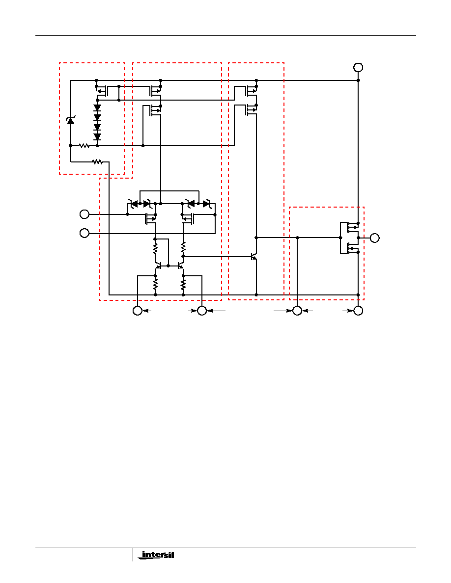
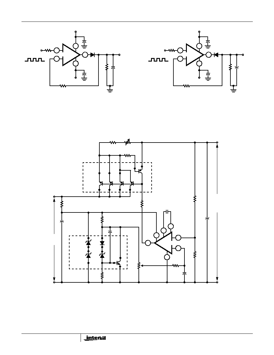
Schematic Diagram
Application Information
Circuit Description
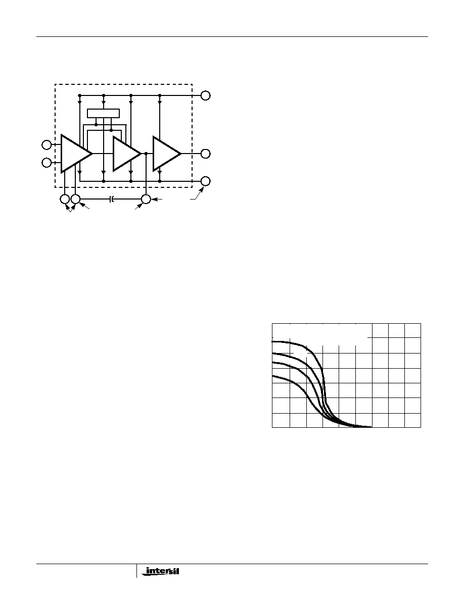
Figure 7 is a block diagram of the HCA10014. The input
terminals may be operated down to 0.5V below the negative
supply rail, and the output can be swung very close to either
supply rail in many applications. Consequently, the
HCA10014 is ideal for single supply operation. Three
Class A amplifier stages, having the individual gain
capability and current consumption shown in Figure 7,
provide the total gain of the HCA10014. A biasing circuit
provides two potentials for common use in the first and
second stages. Terminal 8 can be used both for phase
compensation and to strobe the output stage into
quiescence. When Terminal 8 is tied to the negative supply
rail (Terminal 4) by mechanical or electrical means, the
output potential at Terminal 6 essentially rises to the positive
supply rail potential at Terminal 7. This condition of
essentially zero current drain in the output stage under the
strobed "OFF" condition can only be achieved when the
ohmic load resistance presented to the amplifier is very high
(e.g., when the amplifier output is used to drive CMOS digital
circuits in Comparator applications).
Input Stage
The circuit is shown in the schematic diagram. It consists of
a differential input stage using PMOS field effect transistors
(Q
6
, Q
7
) working into a mirror pair of bipolar transistors (Q
9
,
Q
10
) functioning as load resistors together with resistors R
3
through R
6
. The mirror pair transistors also function as a
differential to single ended converter to provide base drive to
the second stage bipolar transistor (Q
11
). Offset nulling,
when desired, can be effected by connecting a 100,000
potentiometer across Terminals 1 and 5 and the
potentiometer slider arm to Terminal 4. Cascade connected
PMOS transistors Q
2
, Q
4
are the constant current source for
the input stage. The biasing circuit for the constant current
source is subsequently described. The small diodes D
5
3
2
1
8
4
6
7
Q
1
Q
2
Q
4
D
1
D
2
D
3
D
4
Q
3
Q
5
D
5
D
6
D
7
D
8
Q
9
Q
10
Q
6
Q
7
5
Z
1
8.3V
INPUT STAGE
R
3
1k
R
4
1k
R
6
1k
R
5
1k
NON-INV.
INPUT
INV.-INPUT
+
-
R
1
40k
5k
R
2
BIAS CIRCUIT
CURRENT SOURCE FOR
"CURRENT SOURCE
LOAD" FOR Q
11
Q
6
AND Q
7
V+
OUTPUT
OUTPUT
STAGE
Q
8
Q
12
V-
Q
11
SECOND
STAGE
OFFSET NULL
COMPENSATION
STROBING
(NOTE 4)
NOTE:
4. Diodes D
5
through D
8
provide gate-oxide protection for MOSFET input stage.
HCA10014
6
through D
8
provide gate oxide protection against high
voltage transients, including static electricity during handling
for Q
6
and Q
7
.
Second Stage
Most of the voltage gain is provided by the second amplifier
stage, consisting of bipolar transistor Q
11
and its cascade
connected load resistance provided by PMOS transistors Q
3
and Q
5
. The source of bias potentials for these PMOS
transistors is subsequently described. Miller Effect
compensation (roll off) is accomplished by simply connecting
a small capacitor between Terminals 1 and 8. A 47pF
capacitor provides sufficient compensation for stable unity
gain operation in most applications.
Bias Source Circuit
At total supply voltages, somewhat above 8.3V, resistor R
2
and zener diode Z
1
serve to establish a voltage of 8.3V
across the series connected circuit, consisting of resistor R
1
,
diodes D
1
through D
4
, and PMOS transistor Q
1
. A tap at the
junction of resistor R
1
and diode D
4
provides a gate bias
potential of about 4.5V for PMOS transistors Q
4
and Q
5
with
respect to Terminal 7. A potential of about 2.2V is developed
across diode connected PMOS transistor Q
1
with respect to
Terminal 7 to provide gate bias for PMOS transistors Q
2
and
Q
3
. It should be noted that Q
1
is "mirror connected (see
Note 7)" to both Q
2
and Q
3
. Since transistors Q
1
, Q
2
, Q
3
are
designed to be identical, the approximately 200
µ
A current in
Q
1
establishes a similar current in Q
2
and Q
3
as constant
current sources for both the first and second amplifier
stages, respectively.
At total supply voltages somewhat less than 8.3V, zener
diode Z
1
becomes nonconductive and the potential,
developed across series connected R
1
, D
1
-D
4
, and Q
1
,
varies directly with variations in supply voltage.
Consequently, the gate bias for Q
4
, Q
5
and Q
2
, Q
3
varies in
accordance with supply voltage variations. This variation
results in deterioration of the power supply rejection ratio
(PSRR) at total supply voltages below 8.3V. Operation at
total supply voltages below about 4.5V results in seriously
degraded performance.
Output Stage
The output stage consists of a drain loaded inverting
amplifier using CMOS transistors operating in the Class A
mode. When operating into very high resistance loads, the
output can be swung within millivolts of either supply rail.
Because the output stage is a drain loaded amplifier, its gain
is dependent upon the load impedance. The transfer
characteristics of the output stage for a load returned to the
negative supply rail are shown in Figure 8. Typical op amp
loads are readily driven by the output stage. Because large
signal excursions are nonlinear, requiring feedback for good
waveform reproduction, transient delays may be
encountered. As a voltage follower, the amplifier can achieve
0.01% accuracy levels, including the negative supply rail.
NOTE:
7. For general information on the characteristics of CMOS transistor
pairs in linear circuit applications, see Document # 619, data
sheet on CA3600E "CMOS Transistor Array".
Input Current Variation with Common Mode Input
Voltage
As shown in the Table of Electrical Specifications, the input
current for the HCA10014 is typically 5pA at T
A
= 25
o
C when
Terminals 2 and 3 are at a common mode potential of +7.5V
with respect to negative supply Terminal 4. Figure 9 contains
data showing the variation of input current as a function of
3
2
7
4
8
1
5
6
BIAS CKT.
COMPENSATION
(WHEN REQUIRED)
A
V
5X
A
V
A
V
6000X
30X
INPUT
+
-
200
µ
A
200
µ
A
1.35mA
8mA
0mA
V+
OUTPUT
V-
STROBE
C
C
OFFSET
NULL
HCA10014
(NOTE 6)
(NOTE 5)
NOTES:
5. Total supply voltage (for indicated voltage gains) = 15V with input
terminals biased so that Terminal 6 potential is +7.5V above
Terminal 4.
6. Total supply voltage (for indicated voltage gains) = 15V with
output terminal driven to either supply rail.
FIGURE 7. BLOCK DIAGRAM OF THE HCA10014
22.5
GATE VOLTAGE (TERMINALS 4 AND 8) (V)
OUTPUT V
O
L
T
A
GE (TERMINALS 4 AND 8) (V)
17.5
20
12.5
15
10
7.5
2.5
5
0
2.5
7.5
5
10
15
12.5
17.5
0
SUPPLY VOLTAGE: V+ = 15, V- = 0V
T
A
= 25
o
C
LOAD RESISTANCE = 5k
500
1k
2k
FIGURE 8. VOLTAGE TRANSFER CHARACTERISTICS OF
CMOS OUTPUT STAGE
HCA10014
7
common mode input voltage at T
A
= 25
o
C. These data show
that circuit designers can advantageously exploit these
characteristics to design circuits which typically require an
input current of less than 1pA, provided the common mode
input voltage does not exceed 2V. As previously noted, the
input current is essentially the result of the leakage current
through the gate protection diodes in the input circuit and,
therefore, a function of the applied voltage. Although the
finite resistance of the glass terminal-to-case insulator of the
metal can package also contributes an increment of leakage
current, there are useful compensating factors.
Offset Nulling
Offset voltage nulling is usually accomplished with a
100,000
potentiometer connected across Terminals 1 and
5 and with the potentiometer slider arm connected to
Terminal 4. A fine offset null adjustment usually can be
effected with the slider arm positioned in the midpoint of the
potentiometer's total range.
Input Current Variation with Temperature
The input current of the HCA10014 circuit is typically 5pA at
25
o
C. The major portion of this input current is due to
leakage current through the gate protective diodes in the
input circuit. As with any semiconductor junction device,
including op amps with a junction FET input stage, the
leakage current approximately doubles for every 10
o
C
increase in temperature. Figure 10 provides data on the
typical variation of input bias current as a function of
temperature.
Input Offset Voltage (VIO) Variation with DC Bias
and Device Operating Life
It is well known that the characteristics of a MOSFET device
can change slightly when a DC gate source bias potential is
applied to the device for extended time periods. The
magnitude of the change is increased at high temperatures.
Users should be alert to the possible impacts of this effect if
the application of the device involves extended operation at
high temperatures with a significant differential DC bias
voltage applied across Terminals 2 and 3. Figure 11 shows
typical data pertinent to shifts in offset voltage encountered
with devices during life testing. At lower temperatures (metal
can and plastic), for example at 85
o
C, this change in voltage
is considerably less. In typical linear applications where the
differential voltage is small and symmetrical, these
incremental changes are of about the same magnitude as
those encountered in an operational amplifier employing a
bipolar transistor input stage. The 2V
DC
differential voltage
example represents conditions when the amplifier output
stage is "toggled", e.g., as in comparator applications.
10
7.5
5
2.5
0
-1
0
1
2
3
4
5
6
7
INPUT CURRENT (pA)
INPUT V
O
L
T
A
GE (V)
T
A
= 25
o
C
3
2
7
4
8
6
PA
V
IN
15V
TO
5V
0V
TO
-10V
V+
V-
FIGURE 9. INPUT CURRENT vs COMMON-MODE VOLTAGE
FIGURE 11. TYPICAL INCREMENTAL OFFSET VOLTAGE
SHIFT vs OPERATING LIFE
V
S
=
±
7.5V
4000
1000
100
10
1
-80
-60
-40
-20
0
20
40
60
80
100 120 140
INPUT CURRENT (pA)
TEMPERATURE (
o
C)
FIGURE 10. INPUT CURRENT vs TEMPERATURE
7
6
5
4
3
2
1
0
500
1000
1500
2000 2500
3000 3500
4000
OFFSET V
O
L
T
A
GE SHIFT (mV)
TIME (HOURS)
DIFFERENTIAL DC VOLTAGE
(ACROSS TERMINALS 2 AND 3) = 0V
OUTPUT VOLTAGE = V+ /2
DIFFERENTIAL DC VOLTAGE
(ACROSS TERMINALS 2 AND 3) = 2V
OUTPUT STAGE TOGGLED
0
HCA10014
8
Power Supply Considerations
Because the HCA10014 is very useful in single supply
applications, it is pertinent to review some considerations
relating to power supply current consumption under both
single and dual supply service. Figures 12A and 12B show
connections for both dual and single supply operation.
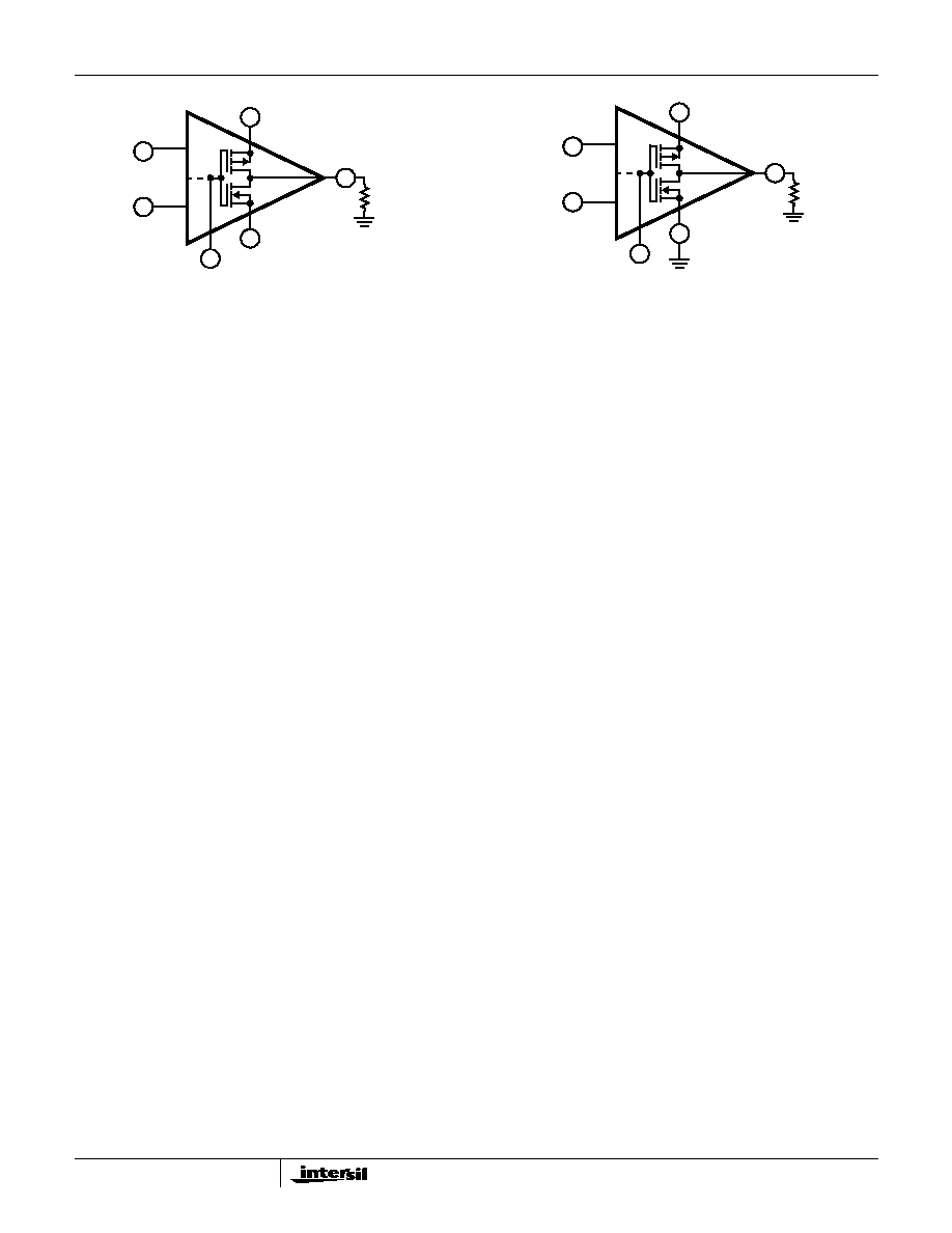
Dual Supply Operation - When the output voltage at
Terminal 6 is 0V, the currents supplied by the two power
supplies are equal. When the gate terminals of Q
8
and Q
12
are driven increasingly positive with respect to ground,
current flow through Q
12
(from the negative supply) to the
load is increased and current flow through Q
8
(from the
positive supply) decreases correspondingly. When the gate
terminals of Q
8
and Q
12
are driven increasingly negative
with respect to ground, current flow through Q
8
is increased
and current flow through Q
12
is decreased accordingly.
Single Supply Operation - Initially, let it be assumed that
the value of R
L
is very high (or disconnected), and that the
input terminal bias (Terminals 2 and 3) is such that the
output terminal (No. 6) voltage is at V+/2, i.e., the voltage
drops across Q
8
and Q
12
are of equal magnitude. Figure 4
shows typical quiescent supply current vs supply voltage for
the HCA10014 operated under these conditions. Since the
output stage is operating as a Class A amplifier, the supply
current will remain constant under dynamic operating
conditions as long as the transistors are operated in the
linear portion of their voltage transfer characteristics (see
Figure 8). If either Q
8
or Q
12
are swung out of their linear
regions toward cutoff (a nonlinear region), there will be a
corresponding reduction in supply current. In the extreme
case, e.g., with Terminal 8 swung down to ground potential
(or tied to ground), NMOS transistor Q
12
is completely cut
off and the supply current to series connected transistors
Q
8
, Q
12
goes essentially to zero. The two preceding stages,
however, continue to draw modest supply current (see the
lower curve in Figure 4) even though the output stage is
strobed off. Figure 12A shows a dual supply arrangement for
the output stage that can also be strobed off, assuming
R
L
=
by pulling the potential of Terminal 8 down to that of
Terminal 4.
Let it now be assumed that a load resistance of nominal
value (e.g., 2k
) is connected between Terminal 6 and
ground in the circuit of Figure 12B. Let it be assumed again
that the input terminal bias (Terminals 2 and 3) is such that
the output terminal (No. 6) voltage is at V+/2. Since PMOS
transistor Q
8
must now supply quiescent current to both R
L
and transistor Q
12
, it should be apparent that under these
conditions the supply current must increase as an inverse
function of the R
L
magnitude. Figure 5 shows the voltage
drop across PMOS transistor Q
8
as a function of load
current at several supply voltages. Figure 8 shows the
voltage transfer characteristics of the output stage for
several values of load resistance.
Wideband Noise
From the standpoint of low noise performance
considerations, the use of the HCA10014 is most
advantageous in applications where the source resistance
of the input signal is on the order of 1M
or more. In this
case, the total input referred noise voltage is typically only
23
µ
V when the test circuit amplifier of Figure 13 is
operated at a total supply voltage of 15V. This value of total
input referred noise remains essentially constant, even
though the value of source resistance is raised by an order
of magnitude. This characteristic is due to the fact that
reactance of the input capacitance becomes a significant
factor in shunting the source resistance. It should be noted,
however, that for values of source resistance very much
greater than 1M
, the total noise voltage generated can be
dominated by the thermal noise contributions of both the
feedback and source resistors.
FIGURE 12A. DUAL POWER SUPPLY OPERATION
FIGURE 12B. SINGLE POWER SUPPLY OPERATION
FIGURE 12. OUTPUT STAGE IN DUAL AND SINGLE POWER SUPPLY OPERATION
3
2
8
4
7
6
R
L
Q
8
Q
12
+
-
V+
V-
3
2
8
4
7
6
R
L
Q
8
Q
12
+
-
V+
HCA10014
9
Typical Applications
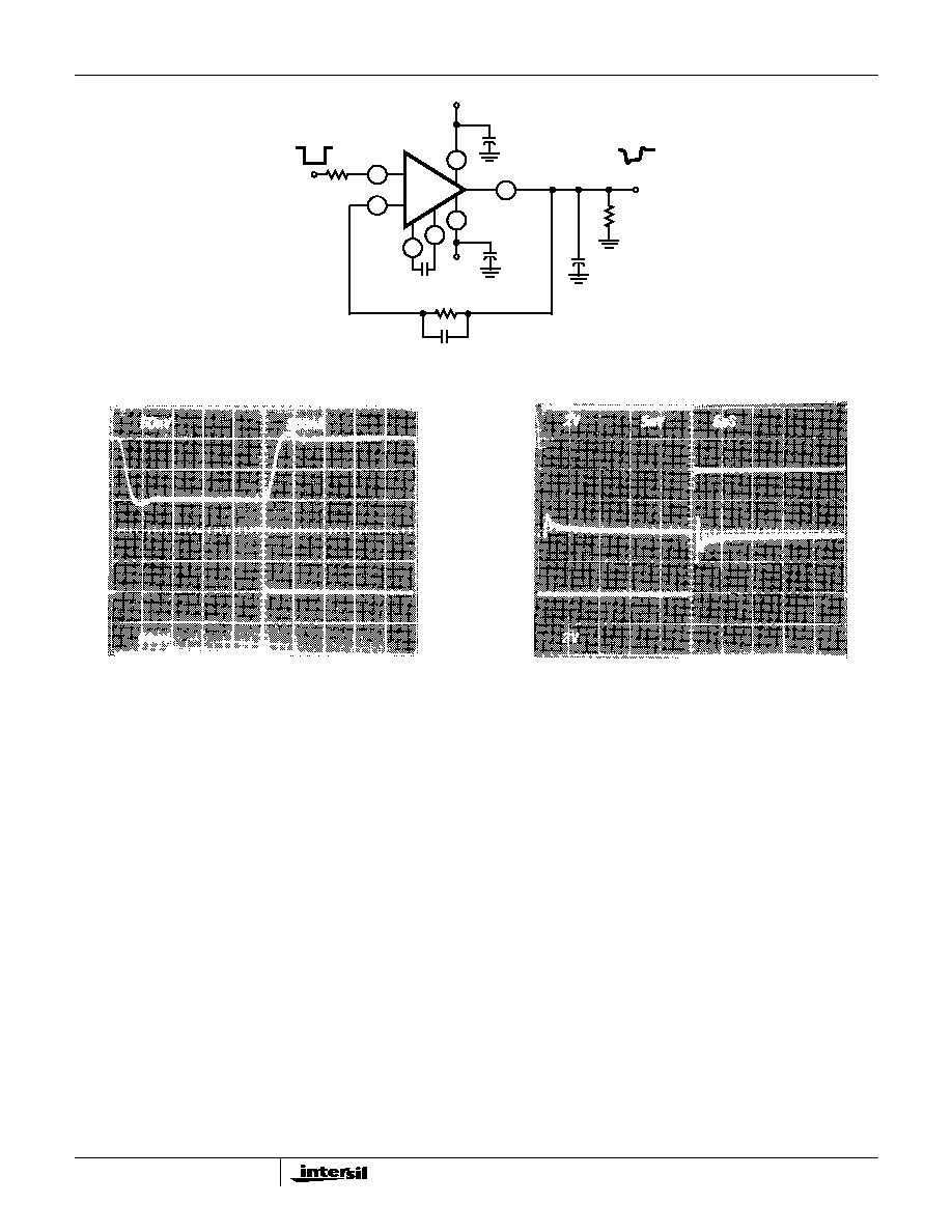
Voltage Followers
Operational amplifiers with very high input resistances are
particularly suited to service as voltage followers. Figure 14
shows the circuit of a classical voltage follower, together with
pertinent waveforms in a split supply configuration.
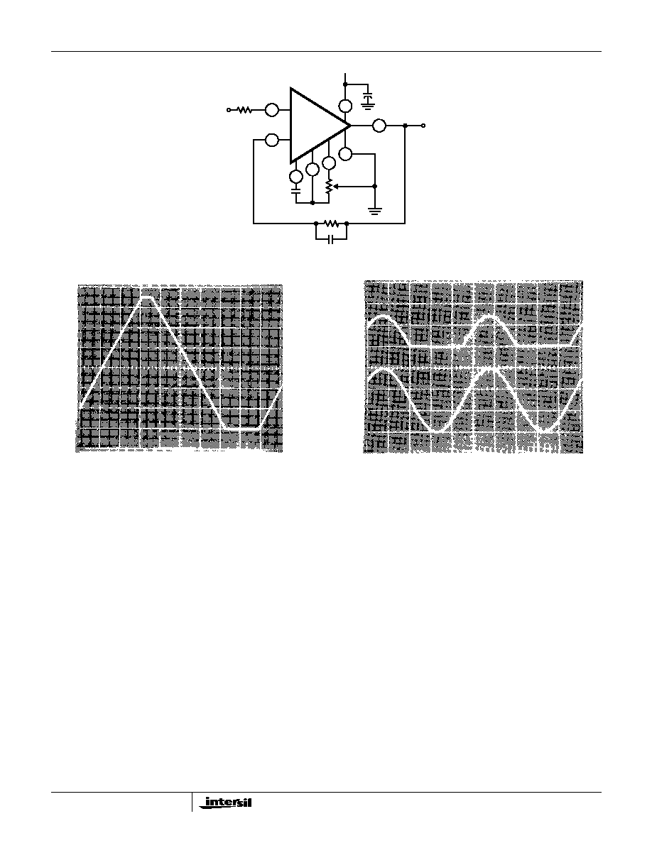
A voltage follower, operated from a single supply, is shown in
Figure 15, together with related waveforms. This follower
circuit is linear over a wide dynamic range, as illustrated by
the reproduction of the output waveform in Figure 15A with
input signal ramping. The waveforms in Figure 15B show
that the follower does not lose its input to output phase
sense, even though the input is being swung 7.5V below
ground potential. This unique characteristic is an important
attribute in both operational amplifier and comparator
applications. Figure 15B also shows the manner in which the
CMOS output stage permits the output signal to swing down
to the negative supply rail potential (i.e., ground in the case
shown). The digital-to-analog converter (DAC) circuit,
described later, illustrates the practical use of the HCA10014
in a single supply voltage follower application.
9-Bit CMOS DAC
A typical circuit of a 9-bit Digital-to-Analog Converter (DAC)
is shown in Figure 16. This system combines the concepts of
multiple switch CMOS lCs, a low cost ladder network of
discrete metal oxide film resistors, a HCA10014 op amp
connected as a follower, and an inexpensive monolithic
regulator in a simple single power supply arrangement. An
additional feature of the DAC is that it is readily interfaced
with CMOS input logic, e.g., 10V logic levels are used in the
circuit of Figure 16.
The circuit uses an R/2R voltage ladder network, with the
output potential obtained directly by terminating the ladder
arms at either the positive or the negative power supply
terminal. Each CD4007A contains three "inverters", each
"inverter" functioning as a single pole double throw switch to
terminate an arm of the R/2R network at either the positive
or negative power supply terminal. The resistor ladder is an
assembly of 1% tolerance metal oxide film resistors. The five
arms requiring the highest accuracy are assembled with
series and parallel combinations of 806,000
resistors from
the same manufacturing lot.
A single 15V supply provides a positive bus for the follower
amplifier and feeds the CA3085 voltage regulator. A
"scale-adjust" function is provided by the regulator output
control, set to a nominal 10V level in this system. The line
voltage regulation (approximately 0.2%) permits a 9-bit
accuracy to be maintained with variations of several volts in
the supply. The flexibility afforded by the CMOS building
blocks simplifies the design of DAC systems tailored to
particular needs.
Single Supply, Absolute Value, Ideal Full Wave
Rectifier
An absolute value circuit is shown in Figure 17. During
positive excursions, the input signal is fed through the
feedback network directly to the output. Simultaneously, the
positive excursion of the input signal also drives the output
terminal (No. 6) of the inverting amplifier in a negative going
excursion such that the 1N914 diode effectively disconnects
the amplifier from the signal path. During a negative going
excursion of the input signal, the HCA10014 functions as a
normal inverting amplifier with a gain equal to -R
2
/R
1
. When
the equality of the two equations shown in Figure 17 is
satisfied, the full wave output is symmetrical.
Peak Detectors
Peak detector circuits are easily implemented, as illustrated
in Figure 18 for both the peak positive and the peak negative
circuit. It should be noted that with large signal inputs, the
bandwidth of the peak negative circuit is much less than that
of the peak positive circuit. The second stage of the
HCA10014 limits the bandwidth in this case. Negative going
output signal excursion requires a positive going signal
excursion at the collector of transistor Q
11
, which is loaded
by the intrinsic capacitance of the associated circuitry in this
mode. On the other hand, during a negative going signal
excursion at the collector of Q
11
, the transistor functions in
an active "pull down" mode so that the intrinsic capacitance
can be discharged more expeditiously.
3
2
1
8
4
7
6
+
-
R
s
1M
47pF -7.5V
0.01
µ
F
+7.5V
0.01
µ
F
NOISE
VOLTAGE
OUTPUT
30.1k
1k
BW (-3dB) = 200kHz
TOTAL NOISE VOLTAGE (REFERRED
TO INPUT) = 23
µ
V (TYP)
FIGURE 13. TEST CIRCUIT AMPLIFIER (30dB GAIN) USED
FOR WIDEBAND NOISE MEASUREMENTS
HCA10014
10
Top Trace: Output
Center Trace: Input
FIGURE 14A. SMALL SIGNAL RESPONSE (50mV/DIV.,
200ns/DIV.)
Top Trace: Output Signal; 2V/Div., 5
µ
s/Div.
Center Trace: Difference Signal; 5mV/Div., 5
µ
s/Div.
Bottom Trace: Input Signal; 2V/Div., 5
µ
s/Div.
FIGURE 14B. INPUT OUTPUT DIFFERENCE SIGNAL SHOWING
SETTLING TIME (MEASUREMENT MADE WITH
TEKTRONIX 7A13 DIFFERENTIAL AMPLIFIER)
FIGURE 14. SPLIT SUPPLY VOLTAGE FOLLOWER WITH ASSOCIATED WAVEFORMS
3
2
1
8
4
7
6
+
-
10k
C
C
= 56pF
-7.5V
0.01
µ
F
+7.5V
0.01
µ
F
2k
2k
BW (-3dB) = 4MHz
SR = 10V/
µ
s
25pF
0.1
µ
F
HCA10014
11
FIGURE 15A. OUTPUT WAVEFORM WITH INPUT SIGNAL
RAMPING (2V/DIV., 500
µ
s/DIV.)
Top Trace: Output; 5V/Div., 200
µ
s/Div.
Bottom Trace: Input Signal; 5V/Div., 200
µ
s/Div.
FIGURE 15B. OUTPUT WAVEFORM WITH GROUND
REFERENCE SINEWAVE INPUT
FIGURE 15. SINGLE SUPPLY VOLTAGE FOLLOWER WITH ASSOCIATED WAVEFORMS. (e.g., FOR USE IN SINGLE SUPPLY D/A
CONVERTER; SEE FIGURE 9 IN AN6080)
3
2
8
1
4
7
6
+
-
10k
56pF
OFFSET
+15V
0.01
µ
F
2k
0.1
µ
F
5
ADJUST
100k
HCA10014

12
FIGURE 16. 9-BIT DAC USING CMOS DIGITAL SWITCHES AND HCA10014
FIGURE 17. SINGLE SUPPLY, ABSOLUTE VALUE, IDEAL FULL WAVE RECTIFIER WITH ASSOCIATED WAVEFORMS
6
3
10
10
3
6
4
8
3
6
7
9
4
10
2
3
13
8
12
12
1
5
8
13
13
1
12
8
5
14
11
2
6
5
1
7
7
1
6
8
4
3
2
10V LOGIC INPUTS
+10.010V
LSB
9
8
7
6
5
4
3
2
1
MSB
806K
1%
PARALLELED
RESISTORS
+15V
VOLTAGE
FOLLOWER
OUTPUT
LOAD
100K
OFFSET
NULL
56pF
2K
0.1
µ
F
REGULATED
VOLTAGE
ADJ
22.1k
1%
1K
3.83k
1%
0.001
µ
F
VOLTAGE
REGULATOR
+15V
2
µ
F
25V
+
-
+10.010V
CD4007A
"SWITCHES"
CD4007A
"SWITCHES"
402K
1%
200K
1%
100K
1%
806K
1%
806K
1%
806K
1%
750K
1%
806K
1%
806K
1%
806K
1%
806K
1%
(2)
(4)
(8)
806K
1%
+
-
62
BIT
1
2
3
4
5
6 - 9
REQUIRED
RATIO MATCH
STANDARD
±
0.1%
±
0.2%
±
0.4%
±
0.8%
±
1% ABS
NOTE: All resistances are in ohms.
CD4007A
"SWITCHES"
1
5
10K
CA3085
HCA10014
20V
P-P
Input: BW(-3dB) = 230kHz, DC Output (Avg) = 3.2V
1V
P-P
Input: BW(-3dB) = 130kHz, DC Output (Avg) = 160mV
Gain =
R
2
R
1
-------
= X =
R
3
R
1
+ R
2
+ R
3
--------------------------------------
R
3
= R
1
X + X
2
1 - X
------------------
For X = 0.5:
2K
4k
------------
=
R
2
R
1
-------
R
3
= 4k
0.75
0.5
-----------
= 6k
Top Trace: Output Signal; 2V/Div.
Bottom Trace: Input Signal; 10V/Div.
Time base on both traces: 0.2ms/Div.
0V
0V
2
3
4
6
8
1
5
7
R
2
2k
+15V
0.01
µ
F
1N914
R
3
5.1k
PEAK
ADJUST
2k
100k
OFFSET
ADJUST
20pF
R
1
4k
+
-
HCA10014
HCA10014
13
FIGURE 18A. PEAK POSITIVE DETECTOR CIRCUIT
FIGURE 18B. PEAK NEGATIVE DETECTOR CIRCUIT
FIGURE 18. PEAK DETECTOR CIRCUITS
FIGURE 19. VOLTAGE REGULATOR CIRCUIT (0V TO 13V AT 40mA)
3
2
6
4
7
+7.5V
0.01
µ
F
+DC
OUTPUT
5
µ
F
+
-
100
k
1N914
0.01
µ
F
-7.5V
2k
10k
+
-
6V
P-P
INPUT;
BW (-3dB) = 1.3MHz
0.3V
P-P
INPUT;
BW (-3dB) = 240kHz
HCA10014
3
2
6
4
7
+7.5V
0.01
µ
F
-DC
OUTPUT
5
µ
F
+
-
100
k
1N914
0.01
µ
F
-7.5V
2k
10k
+
-
6V
P-P
INPUT;
BW (-3dB) = 360kHz
0.3V
P-P
INPUT;
BW (-3dB) = 320kHz
HCA10014
6
3
2
1
8
7
4
CA3086
CURRENT
LIMIT
ADJ
3
R
2
1k
Q
5
13
14
12
Q
1
Q
2
Q
3
Q
4
10
7
3
4
2
6
9
11
8
1
5
390
1k
20k
+
-
5
µ
F
25V
56pF
ERROR
AMPLIFIER
30k
100k
IC1
0.01
µ
F
VOLTAGE
ADJUST
50k
R
1
14
13
Q
5
12
62k
IC
3
OUTPUT
0 TO 13V
AT
40mA
+
-
0.01
µ
F
+20V
INPUT
2.2k
+
-
25
µ
F
IC
2
CA3086 10
11 1, 2
Q
4
Q
1
8, 7
5
Q
3
Q
2
6
4
REGULATION (NO LOAD TO FULL LOAD): <0.01%
INPUT REGULATION: 0.02%/V
HUM AND NOISE OUTPUT: <25
µ
V UP TO 100kHz
+
-
+
-
1k
9
3
HCA10014
HCA10014
14
Error Amplifier in Regulated Power Supplies
The HCA10014 is an ideal choice for error amplifier service
in regulated power supplies since it can function as an error
amplifier when the regulated output voltage is required to
approach zero. Figure 19 shows the schematic diagram of a
40mA power supply capable of providing regulated output
voltage by continuous adjustment over the range from 0V to
13V. Q
3
and Q
4
in lC
2
(a CA3086 transistor array lC)
function as zeners to provide the supply voltage for
comparator IC
1
. Q
1
, Q
2
, and Q
5
in IC
2
are configured as a
low impedance, temperature compensated source of
adjustable reference voltage for the error amplifier.
Transistors Q
1
, Q
2
, Q
3
, and Q
4
in lC
3
(another CA3086
transistor array lC) are connected in parallel as the series
pass element. Transistor Q
5
in lC
3
functions as a current
limiting device by diverting base drive from the series pass
transistors, in accordance with the adjustment of resistor R
2
.
Figure 20 contains the schematic diagram of a regulated
power supply capable of providing regulated output voltage
by continuous adjustment over the range from 0.1V to 50V
and currents up to 1A. The error amplifier (lC
1
) and circuitry
associated with lC
2
function as previously described,
although the output of lC
1
is boosted by a discrete transistor
(Q
4
) to provide adequate base drive for the Darlington
connected series pass transistors Q
1
, Q
2
. Transistor Q
3
functions in the previously described current limiting circuit.
Multivibrators
The exceptionally high input resistance presented by the
HCA10014 is an attractive feature for multivibrator circuit
design because it permits the use of timing circuits with high
R/C ratios. The circuit diagram of a pulse generator (astable
multivibrator), with provisions for independent control of the
"on" and "off" periods, is shown in Figure 21. Resistors R
1
and R
2
are used to bias the HCA10014 to the midpoint of
the supply voltage and R
3
is the feedback resistor. The pulse
repetition rate is selected by positioning S
1
to the desired
position and the rate remains essentially constant when the
resistors which determine "on-period" and "off-period" are
adjusted.
Function Generator
Figure 22 contains a schematic diagram of a function
generator using the HCA10014 in the integrator and
threshold detector functions. This circuit generates a
triangular or square wave output that can be swept over a
1,000,000:1 range (0.1Hz to 100kHz) by means of a single
control, R
1
. A voltage control input is also available for
remote sweep control.
FIGURE 20. VOLTAGE REGULATOR CIRCUIT (0.1V TO 50V AT 1A)
6
2
3
1
8
7
4
4.3k
1
+
-
43k
100
µ
F
ERROR
AMPLIFIER
IC
1
VOLTAGE
ADJUST
14
13
100
µ
F
+55V
INPUT
2.2k
+
-
IC
2
CA3086
10, 11
Q
4
Q
1
Q
2
6
REGULATION (NO LOAD TO FULL LOAD): <0.005%
INPUT REGULATION: 0.01%/V
HUM AND NOISE OUTPUT: <250
µ
V
RMS
UP TO 100kHz
+
-
+
-
+
-
+
-
1W
3.3k
1W
5
µ
F
9
8, 7
Q
3
1, 2
3
5
4
1k
62k
Q
5
12
10k
Q
2
Q
1
50k
Q
3
1k
2N3055
2N2102
CURRENT
LIMIT
ADJUST
2N5294
2N2102
Q
4
1000pF
10k
8.2k
OUTPUT:
0.1 TO 50V
AT 1A
HCA10014
HCA10014
15
The heart of the frequency determining system is an
operational transconductance amplifier (OTA) (see Note 9),
lC
1
, operated as a voltage controlled current source. The
output, I
O
, is a current applied directly to the integrating
capacitor, C
1
, in the feedback loop of the integrator lC
2
,
using a HCA10014, to provide the triangular wave output.
Potentiometer R
2
is used to adjust the circuit for slope
symmetry of positive going and negative going signal
excursions.
Another HCA10014, IC
3
, is used as a controlled switch to
set the excursion limits of the triangular output from the
integrator circuit. Capacitor C
2
is a "peaking adjustment" to
optimize the high frequency square wave performance of the
circuit.
Potentiometer R
3
is adjustable to perfect the "amplitude
symmetry" of the square wave output signals. Output from
the threshold detector is fed back via resistor R
4
to the input
of lC
1
so as to toggle the current source from plus to minus
in generating the linear triangular wave.
Operation with Output Stage Power Booster
The current sourcing and sinking capability of the
HCA10014 output stage is easily supplemented to provide
power boost capability. In the circuit of Figure 23, three
CMOS transistor pairs in a single CA3600E (see Note 11) lC
array are shown parallel connected with the output stage in
the HCA10014. In the Class A mode of CA3600E shown, a
typical device consumes 20mA of supply current at 15V
operation. This arrangement boosts the current handling
capability of the output stage by about 2.5X.
The amplifier circuit in Figure 23 employs feedback to
establish a closed loop gain of 48dB. The typical large signal
bandwidth (-3dB) is 50kHz.
NOTE:
8. See Document # 619 (CA3600E) for technical information.
7
4
6
3
2
R
1
100k
R
2
100k
R
3
100k
ON-PERIOD
ADJUST
1M
2k
2k
OFF-PERIOD
ADJUST
1M
+15V
0.01
µ
F
OUTPUT
2k
0.001
µ
F
0.01
µ
F
0.1
µ
F
1
µ
F
S
1
+
-
FIGURE 21. PULSE GENERATOR (ASTABLE
MULTIVIBRATOR) WITH PROVISIONS FOR
INDEPENDENT CONTROL OF "ON" AND "OFF"
PERIODS
Frequency Range:
Position of S
1
0.001
µ
F
0.01
µ
F
0.1
µ
F
1
µ
F
Pulse Period
4
µ
s to 1ms
40
µ
s to 10ms
0.4ms to 100ms
4ms to 1s
HCA10014
HCA10014
16
NOTE:
9. See Document # 475 (CA3080/CA3080A) and AN6668 for technical information.
FIGURE 22. FUNCTION GENERATOR (FREQUENCY CAN BE VARIED 1,000,000/1 WITH A SINGLE CONTROL)
NOTES:
10. Transistors Q
P1
, Q
P2
, Q
P3
and Q
N1
, Q
N2
, Q
N3
are parallel connected with Q
8
and Q
12
, respectively, of the HCA10014.
11. See Document # 619 (CA3600E).
FIGURE 23. CMOS TRANSISTOR ARRAY (CA3600E) CONNECTED AS POWER BOOSTER IN THE OUTPUT STAGE OF THE HCA10014
6
3
2
1
4
7
5
6
2
3
4
7
8
1
5
4
6
7
3
2
R
4
270k
+7.5V
VOLTAGE CONTROLLED
CURRENT SOURCE
IC
1
3k
3k
10M
+7.5V
R
2
100k
SLOPE
SYMMETRY
ADJUST
VOLTAGE
CONTROLLED
INPUT
-7.5V
10k
10k
R
1
-7.5V
FREQUENCY
ADJUST
(100kHz MAX)
-7.5V
+7.5V
I
O
IC
2
+7.5V
C
1
100pF
INTEGRATOR
-7.5V
56pF
+
-
CA3080A (NOTE 9)
+
-
39k
3 - 30pF
C
2
ADJUST
HIGH FREQ.
DETECTOR
THRESHOLD
150k
IC
3
+7.5V
+
-
R
3
100k
AMPLITUDE
SYMMETRY
ADJUST
22k
-7.5V
HCA10014
HCA10014
8
7
3
2
+15V
2k
+
-
4
10
3
6
4
9
7
6
14
750k
1
µ
F
2
11
13
1
12
5
8
1
µ
F
0.01
µ
F
510k
500
µ
F
Q
P3
Q
N1
Q
N2
Q
N3
Q
P2
Q
P1
CA3600E
A
V(CL)
= 48dB
LARGE SIGNAL
BW (-3 dB) = 50kHz
R
L
= 100
(P
O
= 150mW
AT THD = 10%)
(NOTE 11)
INPUT
HCA10014
1M
HCA10014
17
All Intersil semiconductor products are manufactured, assembled and tested under ISO9000 quality systems certification.
Intersil semiconductor products are sold by description only. Intersil Corporation reserves the right to make changes in circuit design and/or specifications at any time with-
out notice. Accordingly, the reader is cautioned to verify that data sheets are current before placing orders. Information furnished by Intersil is believed to be accurate and
reliable. However, no responsibility is assumed by Intersil or its subsidiaries for its use; nor for any infringements of patents or other rights of third parties which may result
from its use. No license is granted by implication or otherwise under any patent or patent rights of Intersil or its subsidiaries.
For information regarding Intersil Corporation and its products, see web site http://www.intersil.com
Sales Office Headquarters
NORTH AMERICA
Intersil Corporation
P. O. Box 883, Mail Stop 53-204
Melbourne, FL 32902
TEL: (407) 724-7000
FAX: (407) 724-7240
EUROPE
Intersil SA
Mercure Center
100, Rue de la Fusee
1130 Brussels, Belgium
TEL: (32) 2.724.2111
FAX: (32) 2.724.22.05
ASIA
Intersil (Taiwan) Ltd.
7F-6, No. 101 Fu Hsing North Road
Taipei, Taiwan
Republic of China
TEL: (886) 2 2716 9310
FAX: (886) 2 2715 3029
HCA10014
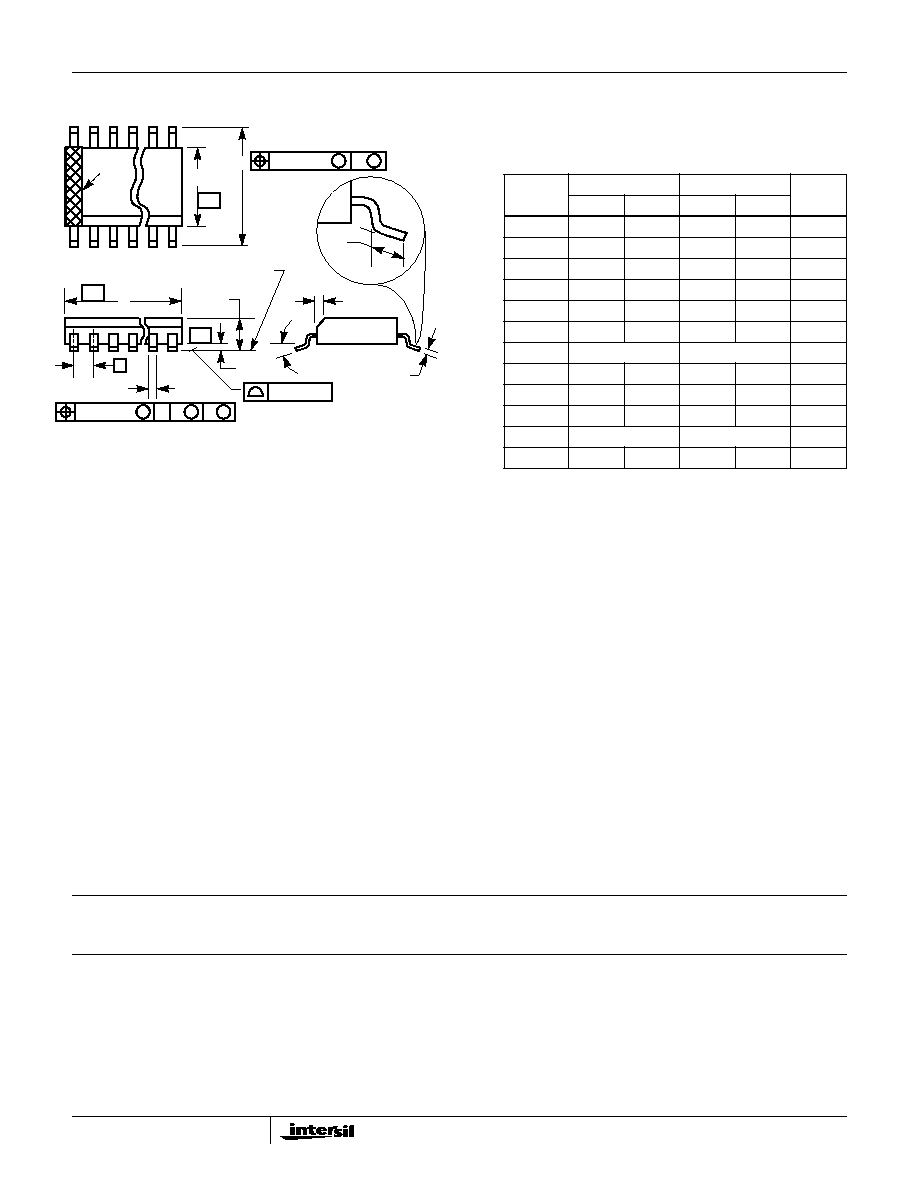
Small Outline Plastic Packages (SOIC)
INDEX
AREA
E
D
N
1
2
3
-B-
0.25(0.010)
C A
M
B S
e
-A-
L
B
M
-C-
A1
A
SEATING PLANE
0.10(0.004)
h x 45
o
C
H
0.25(0.010)
B
M
M
NOTES:
1. Symbols are defined in the "MO Series Symbol List" in Section 2.2 of
Publication Number 95.
2. Dimensioning and tolerancing per ANSI Y14.5M-1982.
3. Dimension "D" does not include mold flash, protrusions or gate burrs.
Mold flash, protrusion and gate burrs shall not exceed 0.15mm (0.006
inch) per side.
4. Dimension "E" does not include interlead flash or protrusions. Inter-
lead flash and protrusions shall not exceed 0.25mm (0.010 inch) per
side.
5. The chamfer on the body is optional. If it is not present, a visual index
feature must be located within the crosshatched area.
6. "L" is the length of terminal for soldering to a substrate.
7. "N" is the number of terminal positions.
8. Terminal numbers are shown for reference only.
9. The lead width "B", as measured 0.36mm (0.014 inch) or greater
above the seating plane, shall not exceed a maximum value of
0.61mm (0.024 inch).
10. Controlling dimension: MILLIMETER. Converted inch dimensions
are not necessarily exact.
M8.15
(JEDEC MS-012-AA ISSUE C)
8 LEAD NARROW BODY SMALL OUTLINE PLASTIC
PACKAGE
SYMBOL
INCHES
MILLIMETERS
NOTES
MIN
MAX
MIN
MAX
A
0.0532
0.0688
1.35
1.75
-
A1
0.0040
0.0098
0.10
0.25
-
B
0.013
0.020
0.33
0.51
9
C
0.0075
0.0098
0.19
0.25
-
D
0.1890
0.1968
4.80
5.00
3
E
0.1497
0.1574
3.80
4.00
4
e
0.050 BSC
1.27 BSC
-
H
0.2284
0.2440
5.80
6.20
-
h
0.0099
0.0196
0.25
0.50
5
L
0.016
0.050
0.40
1.27
6
N
8
8
7
0
o
8
o
0
o
8
o
-
Rev. 0 12/93