 | –≠–ª–µ–∫—Ç—Ä–æ–Ω–Ω—ã–π –∫–æ–º–ø–æ–Ω–µ–Ω—Ç: HFA1145 | –°–∫–∞—á–∞—Ç—å:  PDF PDF  ZIP ZIP |
3-214
CAUTION: These devices are sensitive to electrostatic discharge; follow proper IC Handling Procedures.
http://www.intersil.com or 407-727-9207
|
Copyright
©
Intersil Corporation 1999
HFA1145/883
High Speed, Low Power, Current Feedback Video
Operational Amplifier with Output Disable
Description
The HFA1145/883 is a high speed, low power current
feedback amplifier built with Intersil' proprietary
complementary bipolar UHF-1 process.
This amplifier features a TTL/CMOS compatible disable
control, pin 8, which when pulled low, reduces the supply
current and forces the output into a high impedance state.
This allows easy implementation of simple, low power video
switching and routing systems. Component and composite
video systems also benefit from this op amp's excellent gain
flatness, and good differential gain and phase specifications.
Multiplexed A/D applications will also find the HFA1145/883
useful as the A/D driver/multiplexer.
The HFA1145/883 is a low power, high performance upgrade
for the CLC410.
Ordering Information
PART NUMBER
TEMPERATURE
RANGE
PACKAGE
HFA1145MJ/883
-55
o
C to +125
o
C
8 Lead CerDIP
Features
∑ This Circuit is Processed in Accordance to MIL-STD-
883 and is Fully Conformant Under the Provisions of
Paragraph 1.2.1.
∑ Low Supply Current. . . . . . . . . . . . . . . . . . 5.9mA (Typ)
∑ Wide -3dB Bandwidth . . . . . . . . . . . . . . . 360MHz (Typ)
∑ High Slew Rate . . . . . . . . . . . . . . . . . . . . 1000V/
µ
s (Typ)
∑ Excellent Gain Flatness (to 50MHz)
. . . . .±
0.07dB (Typ)
∑ Excellent Differential Gain . . . . . . . . . . . . . 0.02% (Typ)
∑ Excellent Differential Phase . . . . . . . . . 0.03 Deg. (Typ)
∑ High Output Current . . . . . . . . . . . . . . . . . . 60mA (Typ)
∑ Output Enable / Disable Time . . . . . . 180ns/35ns (Typ)
Applications
∑ Multiplexed Flash A/D Driver
∑ RGB Multiplexers / Preamps for Multimedia Systems
∑ Video Switching and Routing
∑ Pulse and Video Amplifiers
∑ Wideband Amplifiers
∑ RF/IF Signal Processing
∑ Medical Imaging Systems
June 1994
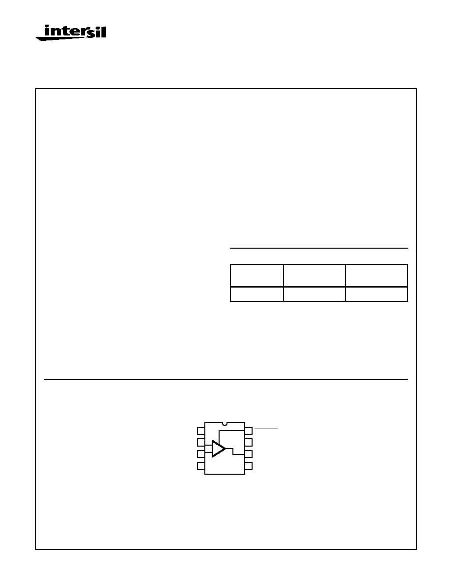
Pinout
HFA1145/883
(CERDIP)
TOP VIEW
NC
-IN
+IN
V-
1
2
3
4
8
7
6
5
DISABLE
V+
OUT
NC
+
-
Spec Number
511116-883
File Number
3726
3-215
Specifications HFA1145/883
Absolute Maximum Ratings
Thermal Information
Voltage Between V+ and V- . . . . . . . . . . . . . . . . . . . . . . . . . . . . 12V
Differential Input Voltage . . . . . . . . . . . . . . . . . . . . . . . . . . . . . . . 5V
Voltage at Either Input Terminal . . . . . . . . . . . . . . . . . . . . . . V+ to V-
Output Current (Note 1) . . . . . . . . . . . . . . . . Short Circuit Protected
Output Current (50% Duty Cycle, Note 1) . . . . . . . . . . . . . . . . 60mA
Junction Temperature . . . . . . . . . . . . . . . . . . . . . . . . . . . . . . +175
o
C
ESD Rating. . . . . . . . . . . . . . . . . . . . . . . . . . . . . . . . . . . . . . > 2000V
Storage Temperature Range . . . . . . . . . . . . . . -65
o
C
T
A
+150
o
C
Lead Temperature (Soldering 10s) . . . . . . . . . . . . . . . . . . . . +300
o
C
Thermal Resistance
JA
JC
CerDIP Package . . . . . . . . . . . . . . . . .
115
o
C/W
30
o
C/W
Maximum Package Power Dissipation at +75
o
C
CerDIP Package . . . . . . . . . . . . . . . . . . . . . . . . . . . . . . . . . 0.87W
Package Power Dissipation Derating Factor above +75
o
C
CerDIP Package . . . . . . . . . . . . . . . . . . . . . . . . . . . . . . 8.7mW/
o
C
CAUTION: Stresses above those listed in "Absolute Maximum Ratings" may cause permanent damage to the device. This is a stress only rating and operation
of the device at these or any other conditions above those indicated in the operational sections of this specification is not implied.
Operating Conditions
Operating V
SUPPLY
(
±
V
S
)
. . . . . . . . . . . . . . . . . . . . . . . . . . . . . . . . . ±
5V
Operating Temperature Range . . . . . . . . . . . . . -55
o
C
T
A
+125
o
C
R
L
50
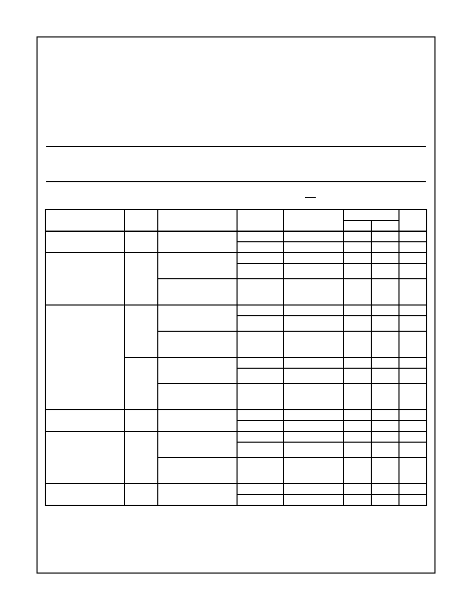
TABLE 1. DC ELECTRICAL PERFORMANCE CHARACTERISTICS
Device Tested at: V
SUPPLY
=
±
5V, A
V
= +1, R
F
= 510
, R
SOURCE
= 0
, R
L
= 100
, V
OUT
= 0V, DIS = Floated, Unless Otherwise Specified.
PARAMETERS
SYMBOL
CONDITIONS
GROUP A
SUBGROUPS
TEMPERATURE
LIMITS
UNITS
MIN
MAX
Input Offset Voltage
V
IO
V
CM
= 0V
1
+25
o
C
-5
5
mV
2, 3
+125
o
C, -55
o
C
-10
10
mV
Common Mode
Rejection Ratio
CMRR
V
CM
=
±
1.8V
V+ = 3.2V, V- = -6.8V
V+ = 6.8V, V- = -3.2V
1
+25
o
C
47
-
dB
2
+125
o
C
44
-
dB
V
CM
=
±
1.2V
V+ = 3.8V, V- = -6.2V
V+ = 6.2V, V- = -3.8V
3
-55
o
C
44
-
dB
Power Supply
Rejection Ratio
PSRRP
V
SUPPLY
=
±
1.8V
V+ = 6.8V, V- = -5V
V+ = 3.2V, V- = -5V
1
+25
o
C
50
-
dB
2
+125
o
C
46
-
dB
V
SUPPLY
=
±
1.2V
V+ = 6.2V, V- = -5V
V+ = 3.8V, V- = -5V
3
-55
o
C
46
-
dB
PSRRN
V
SUPPLY
=
±
1.8V
V+ = 5V, V- = -6.8V
V+ = 5V, V- = -3.2V
1
+25
o
C
50
-
dB
2
+125
o
C
46
-
dB
V
SUPPLY
=
±
1.2V
V+ = 5V, V- = -6.2V
V+ = 5V, V- = -3.8V
3
-55
o
C
46
-
dB
Non-Inverting Input (+IN)
Current
I
BSP
V
CM
= 0V
1
+25
o
C
-15
15
µ
A
2, 3
+125
o
C, -55
o
C
-25
25
µ
A
+IN Current Common
Mode Sensitivity
CMS
IBP
V
CM
=
±
1.8V
V+ = 3.2V, V- = -6.8V
V+ = 6.8V, V- = -3.2V
1
+25
o
C
-
1.25
µ
A/V
2
+125
o
C
-
2.85
µ
A/V
V
CM
=
±
1.2V
V+ = 3.8V, V- = -6.2V
V+ = 6.2V, V- = -3.8V
3
-55
o
C
-
2.85
µ
A/V
+IN Resistance
+R
IN
Note 2
1
+25
o
C
800
-
k
2, 3
+125
o
C, -55
o
C
350
-
k
Spec Number
511116-883
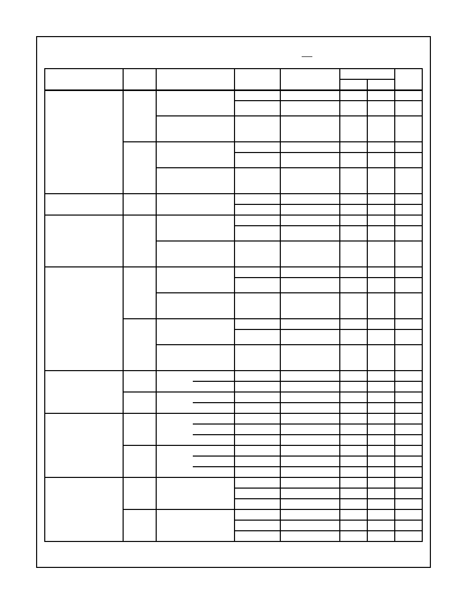
3-216
Specifications HFA1145/883
+IN Current Power
Supply Sensitivity
PPSS
IBP
V
SUPPLY
=
±
1.8V
V+ = 6.8V, V- = -5V
V+ = 3.2V, V- = -5V
1
+25
o
C
-
1
µ
A/V
2
+125
o
C
-
3
µ
A/V
V
SUPPLY
=
±
1.2V
V+ = 6.2V, V- = -5V
V+ = 3.8V, V- = -5V
3
-55
o
C
-
3
µ
A/V
NPSS
IBP
V
SUPPLY
=
±
1.8V
V+ = 5V, V- = -6.8V
V+ = 5V, V- = -3.2V
1
+25
o
C
-
1
µ
A/V
2
+125
o
C
-
3
µ
A/V
V
SUPPLY
=
±
1.2V
V+ = 5V, V- = -6.2V
V+ = 5V, V- = -3.8V
3
-55
o
C
-
3
µ
A/V
Inverting Input (-IN)
Current
I
BSN
V
CM
= 0V
1
+25
o
C
-7.5
7.5
µ
A
2, 3
+125
o
C, -55
o
C
-25
25
µ
A
-IN Current Common
Mode Sensitivity
CMS
IBN
V
CM
=
±
1.8V
V+ = 3.2V, V- = -6.8V
V+ = 6.8V, V- = -3.2V
1
+25
o
C
-
6
µ
A/V
2
+125
o
C
-
8
µ
A/V
V
CM
=
±
1.2V
V+ = 3.8V, V- = -6.2V
V+ = 6.2V, V- = -3.8V
3
-55
o
C
-
8
µ
A/V
-IN Current Power
Supply Sensitivity
PPSS
IBN
V
SUPPLY
=
±
1.8V
V+ = 6.8V, V- = -5V
V+ = 3.2V, V- = -5V
1
+25
o
C
-
5
µ
A/V
2
+125
o
C
-
8
µ
A/V
V
SUPPLY
=
±
1.2V
V+ = 6.2V, V- = -5V
V+ = 3.8V, V- = -5V
3
-55
o
C
-
8
µ
A/V
NPSS
IBN
V
SUPPLY
=
±
1.8V
V+ = 5V, V- = -6.8V
V+ = 5V, V- = -3.2V
1
+25
o
C
-
5
µ
A/V
2
+125
o
C
-
8
µ
A/V
V
SUPPLY
=
±
1.2V
V+ = 5V, V- = -6.2V
V+ = 5V, V- = -3.8V
3
-55
o
C
-
8
µ
A/V
Output Voltage Swing
V
OP100
A
V
= -1
R
L
= 100
V
IN
= -3.2V
1
+25
o
C
3
-
V
V
IN
= -3V
2, 3
+125
o
C, -55
o
C
2.8
-
V
V
ON100
A
V
= -1
R
L
= 100
V
IN
=+3.2V
1
+25
o
C
-
-3
V
V
IN
= +3V
2, 3
+125
o
C, -55
o
C
-
-2.8
V
Output Voltage Swing
V
OP50
A
V
= -1
R
L
= 50
V
IN
= -2.7V
1
+25
o
C
2.5
-
V
V
IN
= -2.25V
2
+125
o
C
2.0
-
V
V
IN
= -2.25V
3
-55
o
C
1.4
-
V
V
ON50
A
V
= -1
R
L
= 50
V
IN
= +2.7V
1
+25
o
C
-
-2.5
V
V
IN
= +2.25V
2
+125
o
C
-
-2.0
V
V
IN
= +2.25V
3
-55
o
C
-
-1.4
V
Output Current
+I
OUT
Note 3
1
+25
o
C
50
-
mA
2
+125
o
C
40
-
mA
3
-55
o
C
28
-
mA
-I
OUT
Note 3
1
+25
o
C
-
-50
mA
2
+125
o
C
-
-40
mA
3
-55
o
C
-
-28
mA
TABLE 1. DC ELECTRICAL PERFORMANCE CHARACTERISTICS
(Continued)
Device Tested at: V
SUPPLY
=
±
5V, A
V
= +1, R
F
= 510
, R
SOURCE
= 0
, R
L
= 100
, V
OUT
= 0V, DIS = Floated, Unless Otherwise Specified.
PARAMETERS
SYMBOL
CONDITIONS
GROUP A
SUBGROUPS
TEMPERATURE
LIMITS
UNITS
MIN
MAX
Spec Number
511116-883
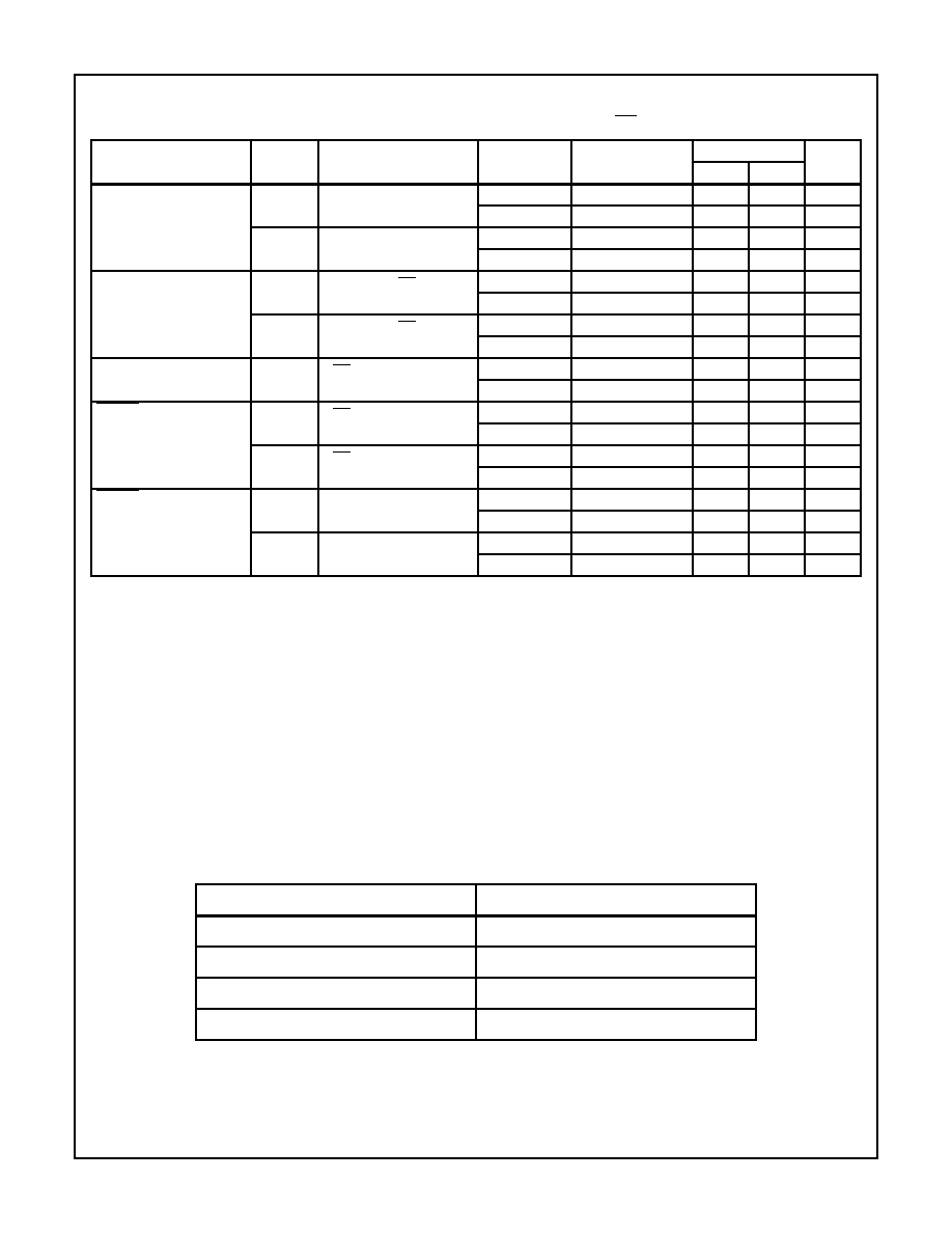
3-217
Specifications HFA1145/883
Quiescent Power
Supply Current
I
CC
R
L
= 100
1
+25
o
C
5.6
6.1
mA
2, 3
+125
o
C, -55
o
C
5.2
6.5
mA
I
EE
R
L
= 100
1
+25
o
C
-6.1
-5.6
mA
2, 3
+125
o
C, -55
o
C
-6.5
-5.2
mA
Disabled Power
Supply Current
DISI
CC
R
L
= 100
,
V
DIS
= 0V
1
+25
o
C
-
4
mA
2, 3
+125
o
C, -55
o
C
-
4
mA
DISI
EE
R
L
= 100
,
V
DIS
= 0V
1
+25
o
C
-4
-
mA
2, 3
+125
o
C, -55
o
C
-4
-
mA
Disabled Output
Leakage Current
DOLC
V
DIS
= 0V,
V
IN
=
±
2.5V, V
OUT
=
2.5V
1
+25
o
C
-10
10
µ
A
2, 3
+125
o
C, -55
o
C
-10
10
µ
A
Disable Input
Current
DILLC
V
DIS
= 0V
1
+25
o
C
-
200
µ
A
2, 3
+125
o
C, -55
o
C
-
200
µ
A
DILHC
V
DIS
= 5V
1
+25
o
C
-
15
µ
A
2, 3
+125
o
C, -55
o
C
-
15
µ
A
Disable Input
Logic Levels
DILLV
1
+25
o
C
-
0.8
V
2, 3
+125
o
C, -55
o
C
-
0.8
V
DILHV
1, 2
+25
o
C, +125
o
C
2.0
-
V
3
-55
o
C
2.4
-
V
NOTES:
1. Output is short circuit protected to ground. Brief short circuits to ground will not degrade reliability, however continuous (100% duty cycle)
output current must not exceed 30mA for maximum reliability.
2. Guaranteed from +IN Common Mode Rejection Test, by: +R
IN
= 1/CMS
IBP
.
3. Guaranteed from V
OUT
Test with R
L
= 50
, by: I
OUT
= V
OUT
/50
.
TABLE 2. AC ELECTRICAL PERFORMANCE CHARACTERISTICS
Table 2 Intentionally Left Blank.
TABLE 3. ELECTRICAL PERFORMANCE CHARACTERISTICS
Table 3 Intentionally Left Blank.
TABLE 4. ELECTRICAL TEST REQUIREMENTS
MIL-STD-883 TEST REQUIREMENTS
SUBGROUPS (SEE TABLE 1)
Interim Electrical Parameters (Pre Burn-In)
1
Final Electrical Test Parameters
1 (Note 1), 2, 3
Group A Test Requirements
1, 2, 3
Groups C and D Endpoints
1
NOTE:
1. PDA applies to Subgroup 1 only.
TABLE 1. DC ELECTRICAL PERFORMANCE CHARACTERISTICS
(Continued)
Device Tested at: V
SUPPLY
=
±
5V, A
V
= +1, R
F
= 510
, R
SOURCE
= 0
, R
L
= 100
, V
OUT
= 0V, DIS = Floated, Unless Otherwise Specified.
PARAMETERS
SYMBOL
CONDITIONS
GROUP A
SUBGROUPS
TEMPERATURE
LIMITS
UNITS
MIN
MAX
+
_
Spec Number
511116-883
3-218
HFA1145/883
Die Characteristics
DIE DIMENSIONS:
59 x 58.2 x 19 mils
±
1 mils
1500 x 1480 x 483
µ
m
±
25.4
µ
m
METALLIZATION:
Type: Metal 1: AICu(2%)/TiW
Type: Metal 2: AICu(2%)
Thickness: Metal 1: 8k
≈
±
0.4k
≈
Thickness: Metal 2: 16k
≈
±
0.8k
≈
GLASSIVATION:
Type: Nitride
Thickness: 4k
≈
±
0.5k
≈
SUBSTRATE POTENTIAL (Powered Up): Floating (Recommend Connection to V-)
WORST CASE CURRENT DENSITY: TBD
TRANSISTOR COUNT: 75
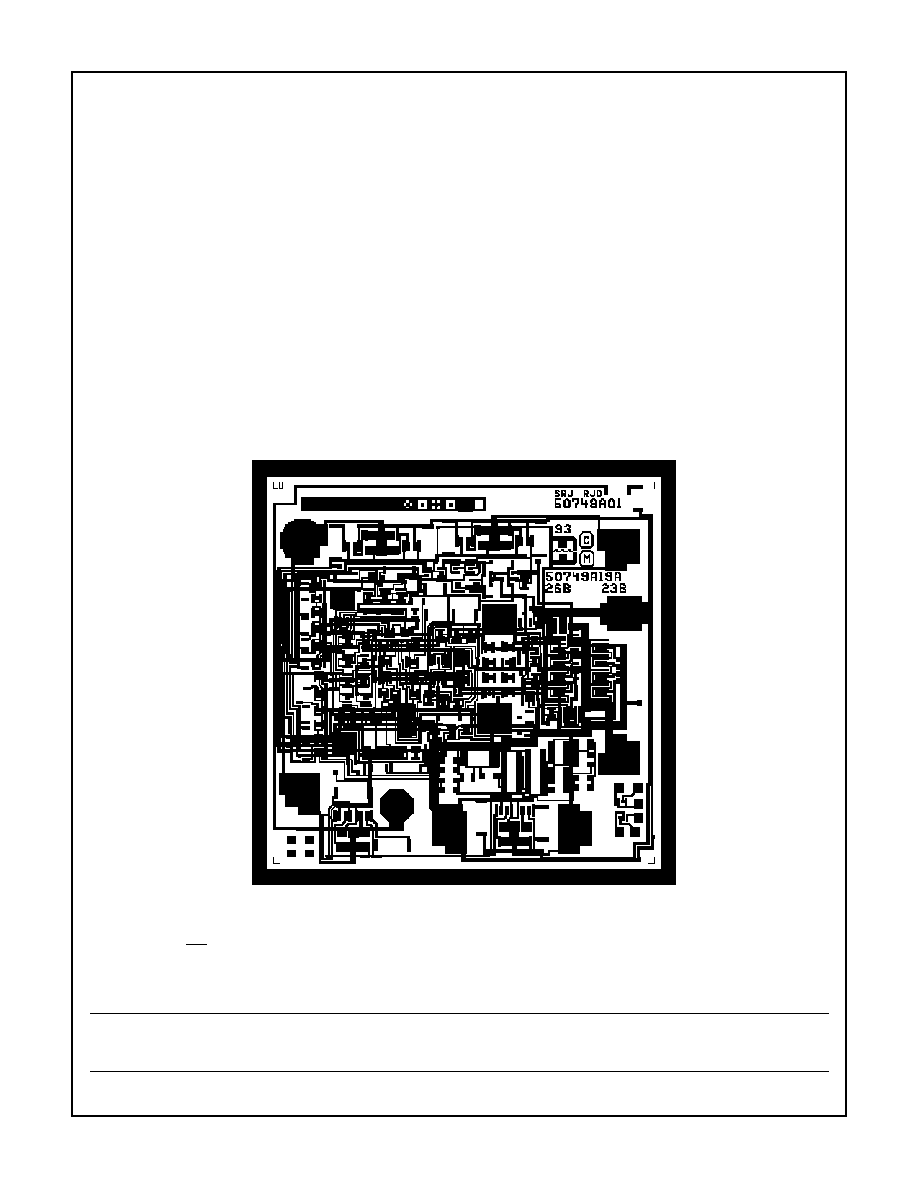
Metallization Mask Layout
HFA1145/883
V-
OPTIONAL
OUT
+IN
-IN
V+
GND (NOTE)
NOTE: This pad is not bonded out on packaged units. Die users may set a GND reference, via this pad, to ensure the TTL compatibility
of the DIS input when using asymmetrical supplies (e.g. V+ = 10V, V- = 0V).
Spec Number
511116-883
All Intersil semiconductor products are manufactured, assembled and tested under ISO9000 quality systems certification.
Intersil products are sold by description only. Intersil Corporation reserves the right to make changes in circuit design and/or specifications at any time without
notice. Accordingly, the reader is cautioned to verify that data sheets are current before placing orders. Information furnished by Intersil is believed to be accurate
and reliable. However, no responsibility is assumed by Intersil or its subsidiaries for its use; nor for any infringements of patents or other rights of third parties which
may result from its use. No license is granted by implication or otherwise under any patent or patent rights of Intersil or its subsidiaries.
For information regarding Intersil Corporation and its products, see web site http://www.intersil.com