
1
HFA3726
400MHz Quadrature IF
Modulator/Demodulator
The HFA3726 is a highly integrated
baseband converter for quadrature
modulation applications. It features all
the necessary functionality for
baseband modulation and
demodulation of I and Q signals. It has a two stage
integrated limiting IF amplifier with 84dB of gain and a built in
Receive Signal Strength Indicator (RSSI). "I" and "Q"
Baseband antialiasing and shaping filters are integrated in
this design. In addition, these filters are continuously tunable
over a
±
10% frequency range via one external resistor. The
modulator channel receives digital I and Q data for
processing. To achieve broadband operation, the Local
Oscillator frequency input is required to be twice the desired
frequency of modulation/demodulation. A selectable
buffered divide by 2 LO output and a stable reference
voltage is provided for convenience of the user. The device is
housed in a thin 80 lead TQFP package well suited for
PCMCIA board applications.
Features
∑ Integrates all IF Transmit and Receive Functions
∑ Broad Frequency Range . . . . . . . . . . . 10MHz to 400MHz
∑ 5th Order Low Pass Filter. . . . . . . . . . . . . . . . . . . .7.7MHz
∑ 400MHz Limiting IF Gain Strip with RSSI. . . . . . . . . .84dB
∑ Low LO Drive Level . . . . . . . . . . . . . . . . . . . . . . . -15dBm
∑ Fast Transmit-Receive Switching . . . . . . . . . . . . . . . . . 1
µ
s
∑ Power Management/Standby Mode
∑ Single Supply 2.7V to 5.5V Operation
Applications
∑ Systems Targeting IEEE 802.11 Standard
∑ TDD Quadrature-Modulated Communication Systems
∑ Wireless Local Area Networks
∑ PCMCIA Wireless Transceivers
∑ ISM Systems
∑ TDMA Packet Protocol Radios
∑ PCS/Wireless PBX
∑ Wireless Local Loop
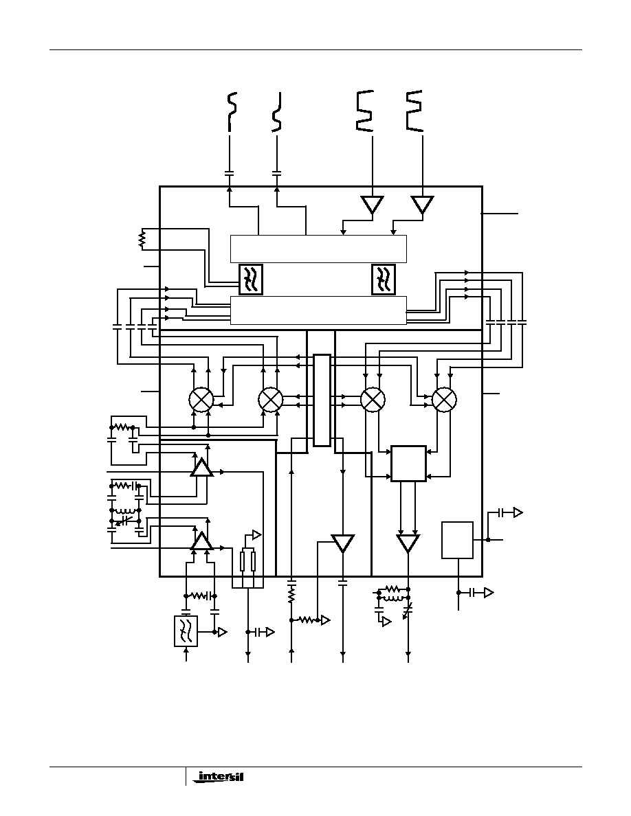
Simplified Block Diagram
Ordering Information
PART NUMBER
TEMP.
RANGE (
o
C)
PACKAGE
PKG. NO.
HFA3726IN
-40 to 85
80 Ld TQFP
Q80.14x14
HFA3726IN96
-40 to 85
80 Ld TQFP
Tape and Reel
TM
LIM1_IN
MOD_LO_IN
MOD_TX_IF_OUT
LIM1_OUT
LIM2_IN
LPF_RXQ _OUT
RSSI2
MOD_LO_OUT
RSSI1
LIM2_OUT
LPF_TUNE_1
LPF_RX_I
LPF_RX_Q
MOD_RX_I
MOD_RX_Q
LPF_TX_Q
MOD_TX_I
MOD_TX_Q
LPF_TX_I
MOD_IF_IN
LPF_TXI_IN
LPF_TXQ_IN
2V
REF
2V REF
LPF_TUNE_0
LPF_RXI_OUT
M
U
X
M
U
X
I
Q
LO_GND
IF
IF
0
o
/90
o
˜
2
November 1999
File Number
4310.3
Data Sheet
CAUTION: These devices are sensitive to electrostatic discharge; follow proper IC Handling Procedures.
1-888-INTERSIL or 321-724-7143
|
Copyright
©
Intersil Corporation 1999
PRISMÆ is a registered trademark of Intersil Corporation. PRISM logo is a trademark of Intersil Corporation.

2
Pinout
80 LEAD TQFP
TOP VIEW
21 22 23 24 25 26 27 28 29 30 31 32 33 34 35 36
1
2
3
4
5
6
7
8
9
10
11
12
13
14
15
16
LPF_RX_PE
LPF_TX_PE
LPF_TXQ-
LPF_RXI+
GND
MOD_RXI-
GND
60
59
58
57
56
55
54
53
52
51
50
49
48
47
46
45
LIM2_RSSI
RSSI_RL2
GND
LIM2_OUT+
LIM2_OUT-
LIM2_V
CC
LIM2_PE
GND
GND
GND
LO_GND
MOD_IF_IN-
MOD IF_IN+
MOD_V
CC
MOD_LO_OUT
MOD_V
CC
64
65
66
67
68
69
70
71
72
73
74
75
76
77
78
79
LIM1_RSSI
RSSI_RL1
GND
LIM1_OUT+
LIM1_OUT
-
LIM1_V
CC
LIM1_PE
GND
GND
GND
GND
GND
GND
GND
GND
GND
63 62 61
LIM2_BYP-
LIM2_IN-
LIM2_IN+
LIM2_BYP+
37 38 39 40
MOD_TXI+
MOD_TXI-
MOD_TXQ+
MOD_TXQ-
MOD_LO_IN
MOD_RX_PE
MOD_TX_IF_OUT
MOD_TX_PE
44
43
42
41
17
18
19
20
80
LPF_TXQ+
LPF_TXI-
LPF_TXI+
LPF_RXQ-
LPF_RXQ+
LPF_RXI-
MOD_RXI+
MOD_RXQ+
MOD_RXQ-
LIM1_BYP+
LIM1_IN+
LIM1_IN-
LIM1_BYP-
GND
GND
GND
GND
LPF_V
CC
2V REF
LPF_TXI_IN
LPF_TXQ_IN
LPF_RXI_OUT
LPF_RXQ_OUT
GND
LPF_BYP
GND
GND
LPF_Tune1
LPF_Tune0
HFA3726
3
Block Diagram
NOTE: V
CC
, GND and Bypass capacitors not shown.
0
o
/
IF
LIM1_IN+
LIM1_IN-
MOD_LO_IN
IF_OUT
LIM1_OUT +
LIM1_OUT -
LIM2_IN-
LIM2_IN+
LPF_RXI_OUT
RSSI_RL1
MOD_LO_OUT
LIM1_RSSI
LIM2_OUT +
LIM2_OUT -
LPF_TUNE1
LPF_RX I +
LPF_RX I -
LPF_RX Q +
LPF_RX Q -
MOD_RX I +
MOD_RX I -
MOD_RX Q +
MOD_RX Q -
MOD_IF_IN +
MOD_IF_IN -
˜
2
LPF_TXI_IN
2V
REF
2V REF
LPF_TUNE0
MOD_TX
LPF_RXQ_OUT
MUX
I
LPF_TX_Q -
MOD TX I +
MOD TX Q -
LPF_TX_Q +
MOD TX Q +
MOD TX I -
LPF_TX_I -
LPF_TX_I +
LPF_TXQ_IN
SA
W
V
CC
50
RSSI
UP CONVER
TER
IF LIMITERS
MUX_LPF
DO
WN CONV
LO_GND
LIM1_PE
LIM2_PE
MOD_RX PE
MOD_TX_PE
LPF_TX_PE
LPF_RX PE
LIM2_RSSI
RSSI_RL2
IF
LPF_BYP
1.25V
IN
(2XLO)
IF
MUX
Q
90
o
HFA3726

4
Pin Description
PIN
SYMBOL
DESCRIPTION
1
LIM1_BYP+
DC feedback pin for Limiter amplifier 1. Requires good decoupling and minimum wire length to a solid signal
ground.
2
LIM1_In+
Non inverting analog input of Limiter amplifier 1.
3
LIM1_In-
Inverting input of Limiter amplifier 1.
4
LIM1_BYP-
DC feedback pin for Limiter amplifier 1. Requires good decoupling and minimum wire length to a solid signal
ground.
5, 6,
7, 8
GND
Ground. Connect to a solid ground plane.
9
LPF_V
CC
Supply pin for the Low pass filter. Use high quality decoupling capacitors right at the pin.
10
2V REF
Stable 2V reference voltage output for external applications. Loading must be higher than 10k
. A bypass
capacitor of at least 0.1
µ
F is required.
11
LPF_BYP
Internal reference bypass pin. This is the common voltage (V
CM
) used for the LPF digital thresholds. Requires
0.1
µ
F decoupling capacitor.
12
LPF_TXI_In
Low pass filter in phase (I) channel transmit digital input. (Note 1)
13
LPF_TXQ_In
Low pass filter quadrature (Q) channel transmit digital input. (Note 1)
14
LPF_RXI_Out
Low pass filter in phase (I) channel receive output. Requires AC coupling. (Note 2)
15
LPF_RXQ_Out
Low pass filter quadrature (Q) channel receive output. Requires AC coupling. (Note 2)
16
GND
Ground. Connect to a solid ground plane.
17
GND
Ground. Connect to a solid ground plane.
18
LPF_Tune1
These two pins are used to fine tune the Low pass filter cutoff frequency. A resistor connected between the two
pins (R
TUNE
) will fine tune both transmit and receive filters. Refer to the tuning equation in the LPF AC
specifications.
19
LPF_Tune0
20
GND
Ground. Connect to a solid ground plane.
21
LPF_RX_PE
Digital input control pin to enable the LPF receive mode of operation. Enable logic level is High.
22
LPF_TX_PE
Digital input control pin to enable the LPF transmit mode of operation. Enable logic level is High.
23
LPF_TXQ-
Negative output of the transmit Low pass filter, quadrature channel. AC coupling is required. Normally connects to
the inverting input of the quadrature Modulator (Mod_TXQ-), pin 40.
24
LPF_TXQ+
Positive output of the transmit Low pass filter, quadrature channel. AC coupling is required. Normally connects to
the non inverting input of the quadrature Modulator (Mod_TXQ+), pin 39.
25
LPF_TXI-
Negative output of the transmit Low pass filter, in phase channel. AC coupling is required. Normally connects to
the inverting input of the in phase Modulator (Mod_TXI-), pin 38.
26
LPF_TXI+
Positive output of the transmit Low pass filter, in phase channel. AC coupling is required. Normally connects to the
non inverting input of the in phase Modulator (Mod_TXI+), pin 37.
27
LPF_RXQ-
Low pass filter inverting input of the receive quadrature channel. AC coupling is required. This input is normally
coupled to the negative output of the quadrature demodulator (Mod_RXQ-), pin 36.
28
LPF_RXQ+
Low pass filter non inverting input of the receive quadrature channel. AC coupling is required. This input is normally
coupled to the positive output of the quadrature demodulator (Mod_RXQ+), pin 35.
29
LPF_RXI-
Low pass filter inverting input of the receive in phase channel. AC coupling is required. This input is normally
coupled to the negative output of the in phase demodulator (Mod_RXI-), pin 34.
30
LPF_RXI+
Low pass filter non inverting input of the receive in phase channel. AC coupling is required. This input is normally
coupled to the positive output of the in phase demodulator (Mod_RXI-), pin 33.
31, 32
GND
Ground. Connect to a solid ground plane.
33
Mod_RXI+
In phase demodulator positive output. AC coupling is required. Normally connects to the non inverting input of the
Low pass filter (LPF_RXI+), pin 30.
34
Mod_RXI-
In phase demodulator negative output. AC coupling is required. Normally connects to the inverting input of the Low
pass filter (LPF_RXI-), pin 29.
HFA3726

5
35
Mod_RXQ+
Quadrature demodulator positive output. AC coupling is required. Normally connects to the non inverting input of
the Low pass filter (LPF_RXQ+), pin 28.
36
Mod_RXQ-
Quadrature demodulator negative output. AC coupling is required. Normally connects to the inverting input of the
Low pass filter (LPF_RXQ+), pin 27.
37
Mod_TXI+
In phase modulator non inverting input. AC coupling is required. This input is normally coupled to the Low pass
filter positive output (LPF_TXI+), pin 26.
38
Mod_TXI-
In phase modulator inverting input. AC coupling is required. This input is normally coupled to the Low pass filter
negative output (LPF_TXI-), pin 25.
39
Mod_TXQ+
Quadrature modulator non inverting input. AC coupling is required. This input is normally coupled to the Low pass
filter positive output (LPF_TXQ+), pin 24.
40
Mod_TXQ-
Quadrature modulator inverting input. AC coupling is required. This input is normally coupled to the Low pass filter
negative output (LPF_TXQ-), pin 23.
41
Mod_TX_PE
Digital input control to enable the Modulator section. Enable logic level is High for transmit.
42
Mod_TX_IF_Out
Modulator open collector output, single ended. Termination resistor to V
CC
with a typical value of 316
.
43
Mod_RX_PE
Digital input control to enable the demodulator section. Enable logic level is High for receive.
44
Mod_LO_In
(2XLO)
Single ended local oscillator current input. Frequency of input signal must be twice the required modulator carrier
and demodulator LO frequency. Input current is optimum at 200
µ
A
RMS
. Input matching networks and filters can
be designed for a wide range of power and impedances at this port. Typical input impedance is 130
.
This pin
requires AC coupling. (Note 3)
NOTE: High second harmonic content input waveforms may degrade I/Q phase accuracy.
45
Mod_V
CC
Modulator/Demodulator supply pin. Use high quality decoupling capacitors right at the pin.
46
Mod_LO_Out
Divide by 2 buffered output reference from "Mod_LO_in" input. Used for external applications where the modulating
and demodulating carrier reference frequency is required. 50
single end driving capability.This output can be
disabled by use of pin 50. AC coupling is required, otherwise tie to V
CC
.
47
Mod_V
CC
Modulator/Demodulator supply pin. Use high quality decoupling capacitors right at the pin.
48
Mod_IF_In+
Demodulator non inverting input. Requires AC coupling.
49
Mod_IF In-
Demodulator inverting input. Requires AC coupling.
50
LO_GND
When grounded, this pin enables the LO buffer (Mod_LO_Out). When open (NC) it disables the LO buffer.
51, 52,
53
GND
Ground. Connect to a solid ground plane.
54
LIM2_PE
Digital input control to enable the limiter amplifier 2. Enable logic level is High.
55
LIM2_V
CC
Limiter amplifier 2 supply pin. Use high quality decoupling capacitors right at the pin.
56
LIM2_Out-
Positive output of limiter amplifier 2. Requires AC coupling.
57
LIM2_Out+
Negative output of limiter amplifier 2. Requires AC coupling.
58
GND
Ground. Connect to a solid ground plane.
59
RSSI_RL2
Load resistor to ground. Nominal value is 6k
. This load is used to terminate the LIM RSSI current output and
maintain temperature and process variation to a minimum.
60
LIM2_RSSI
Current output of RSSI for the limiter amplifier 2. Connect in parallel with the RSSI output of the amplifier limiter 1
for cascaded response.
61
LIM2_BYP+
DC feedback pin for Limiter amplifier 2. Requires good decoupling and minimum wire length to a solid signal
ground.
62
LIM2_In+
Non inverting analog input of Limiter amplifier 2.
63
LIM2_In-
Inverting input of Limiter amplifier 2.
64
LIM2_BYP-
DC feedback pin for Limiter amplifier 2. Requires good decoupling and minimum wire length to a solid signal
ground.
Pin Description
(Continued)
PIN
SYMBOL
DESCRIPTION
HFA3726