 | –≠–ª–µ–∫—Ç—Ä–æ–Ω–Ω—ã–π –∫–æ–º–ø–æ–Ω–µ–Ω—Ç: HFA3763 | –°–∫–∞—á–∞—Ç—å:  PDF PDF  ZIP ZIP |
4-1
File Number
4237.4
HFA3763
400MHz Quadrature Modulator and AGC
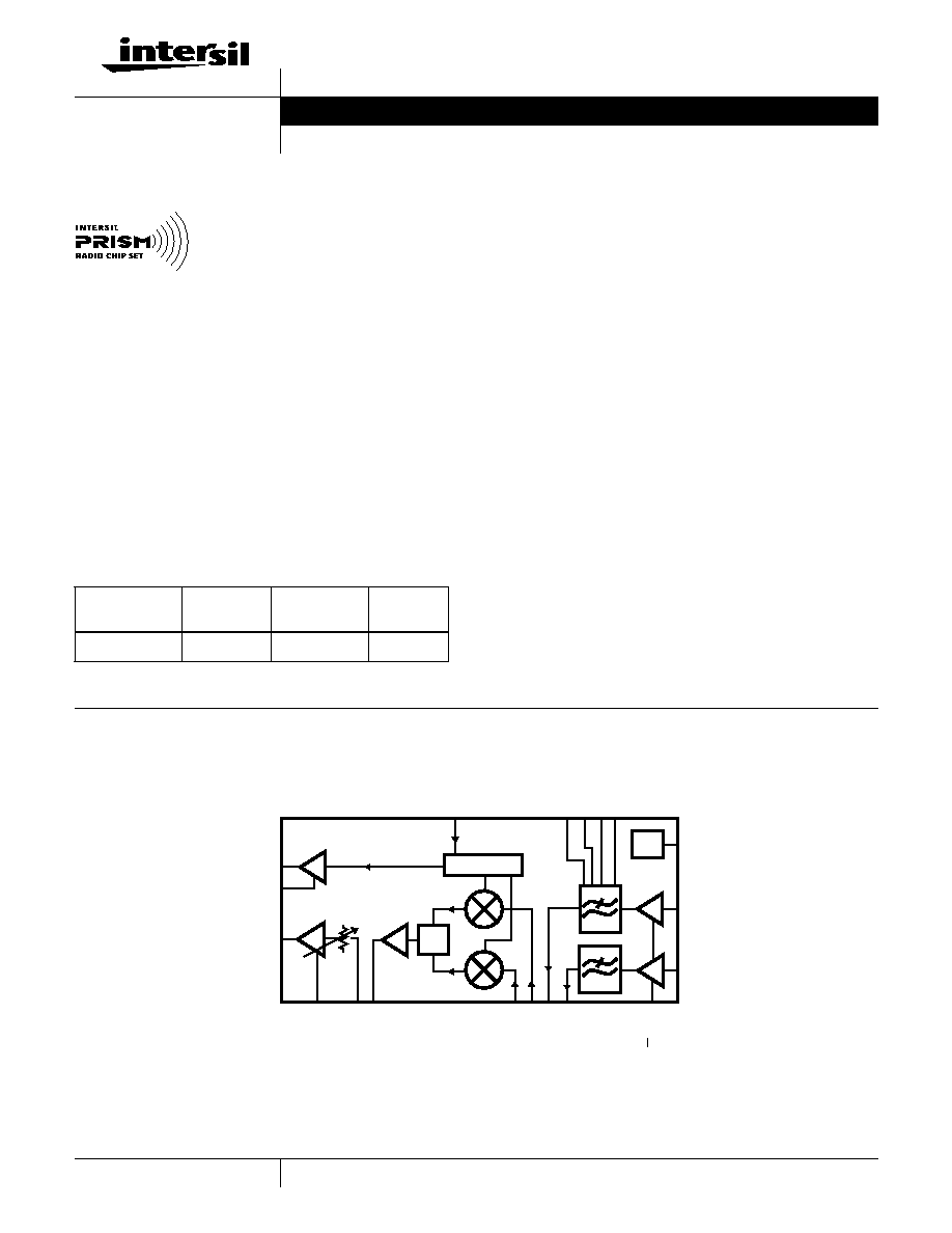
The HFA3763 is a highly integrated
baseband converter for quadrature
modulation applications. The HFA3763
400MHz quadrature modulator and
AGC is one of the seven chips in the
PRISMÆ full duplex chip set (see Typical Application
Diagram). It features all the necessary blocks for baseband
modulation of I and Q signals. An output AGC and Baseband
shaping filters are integrated in the design. Four filter
bandwidths are programmable via a two bit digital control
interface. In addition, these filters are continuously tunable
over a
±
20% frequency range via one external resistor. The
modulator channel receives digital or analog I and Q data for
processing. To achieve broadband operation, the Local
Oscillator frequency input is required to be twice the desired
frequency of modulation. A selectable buffered divide by 2
LO output and a stable reference voltage are provided for
convenience of the user.
Features
∑ Integrates all IF Transmit Functions
∑ Broad Frequency Range . . . . . . . . . . . 10MHz to 400MHz
∑ I/Q Amplitude and Phase Balance . . . . . . . . . . . 0.2dB, 2
o
∑ 5th Order Programmable
Low Pass Filter. . . . . . . . . . . . . . . . . . . 2.2MHz - 17.6MHz
∑ 400MHz Output AGC Amplifier/Attenuator . . . . . . . .45dB
∑ Selectable Digital or Analog TX Baseband Inputs
∑ Low LO Drive Level . . . . . . . . . . . . . . . . . . . . . . . -15dBm
∑ Fast Transmit-on Switching . . . . . . . . . . . . . . . . . . . . . 1
µ
s
∑ Power Management/Standby Mode
∑ Single Supply 2.7V to 5.5V Operation
Applications
∑ Wireless Local Loop Systems
∑ Wireless Local Area Networks
∑ PCMCIA Wireless Duplex Transceivers
∑ ISM Systems
∑ TDMA Packet Protocol Radios
∑ PCS/Wireless PBX
Simplified Block Diagram
Ordering Information
PART NUMBER
TEMP.
RANGE (
o
C)
PACKAGE
PKG. NO.
HFA3763IN
-40 to 85
80 Ld TQFP
Q80.14x14
TM
0
o
/90
o
MOD_LO_IN
MOD_TX_IF_OUT
MOD_LO_OUT
LPF_TUNE_1
LPF_TX_Q
MOD_TX_I
MOD_TX_Q
LPF_TX_I
˜
2
LPF_SEL0
LPF_SEL1
LPF_TXI_IN
LPF_TXQ_IN
2V
REF
2V REF
LPF_TUNE_0
I
Q
LO_GND
IF_OUT
A
GC_CTRL
IF_A
GC_IN
TX
D OR A
Data Sheet
June 1999
CAUTION: These devices are sensitive to electrostatic discharge; follow proper IC Handling Procedures.
http://www.intersil.com or 407-727-9207
|
Copyright
©
Intersil Corporation 1999
PRISMÆ is a registered trademark of Intersil Corporation. PRISM logo is a trademark of Intersil Corporation.
4-2
Pinout
80 LEAD TQFP
TOP VIEW
Typical Application Diagram
21 22 23 24 25 26 27 28 29 30 31 32 33 34 35 36
1
2
3
4
5
6
7
8
9
10
11
12
13
14
15
16
GND
LPF_TX_PE
LPF_TXQ-
GND
GND
60
59
58
57
56
55
54
53
52
51
50
49
48
47
46
45
GND
GND
GND
GND
LO_GND
MOD_BYP
MOD_BYP
MOD_V
CC
MOD_LO_OUT
MOD_V
CC
64
65
66
67
68
69
70
71
72
73
74
75
76
77
78
79
GND
GND
GND
GND
GND
GND
GND
63 62 61
37 38 39 40
MOD_TXI+
MOD_TXI-
MOD_TXQ+
MOD_TXQ-
MOD_LO_IN
GND
MOD_TX_IF_OUT
MOD_TX_PE
44
43
42
41
17
18
19
20
80
LPF_TXQ+
LPF_TXI-
LPF_TXI+
GND
GND
GND
GND
LPF_V
CC
2V REF
LPF_TXI_IN
LPF_TXQ_IN
LPF_SEL1
LPF_SEL0
LPF_TUNE1
LPF_TUNE0
TX D or A
LPF_BYP
IF_AGC_IN
GND
AGC_V
CC
GND
AGC_CTRL
GND
A
GC_V
CC
GND
A
GC_PE
GND
IF_OUT
GND
A
GC_V
CC
GND
GND
GND
GND
GND
GND
GND
GND
GND
GND
NC
NC
NC
NC
NC
NC
NC
NC
NC
NC
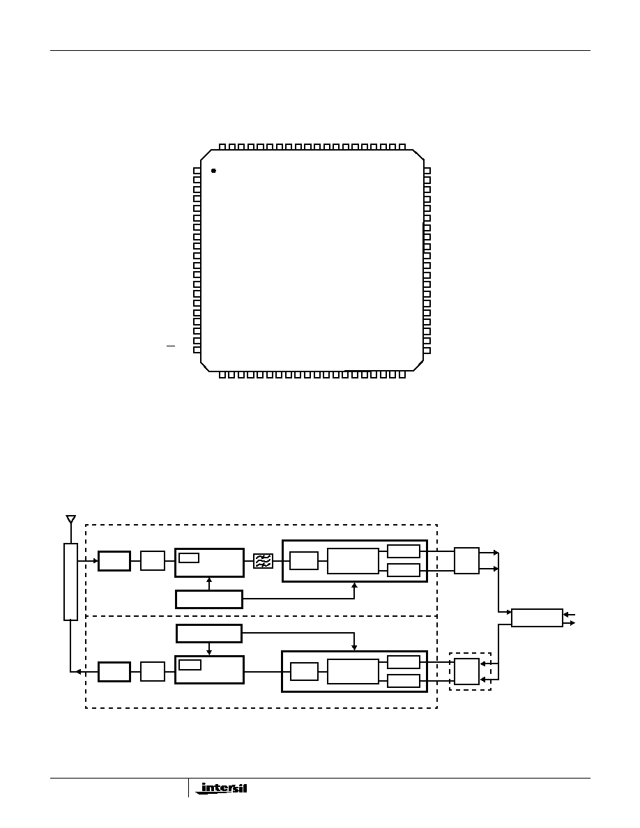
SYNTHESIZER
LNA
BPF
RF/IF
CONVERTER
IF AGC
LPF
QMODEM
IF/RF
CONVERTER
BASEBAND
FILTER
SYNTHESIZER
HFA3424/21
HFA3661
HFA3524
HFA3663 (File #4241)
HFA3925
HFA3761 (File #4236)
HFA3763
LPF
AGC
LPF
QMODEM
LPF
D/A
PA
BPF
HFA3664 (File #4242)
(File #4240)
(File #4062)
HFA3524
(File #4062)
(File #4132)
(File #4131)
(File #4237)
PRISM FULL DUPLEX RADIO
CHIP SET, FILE #4238
A/D
PRISM FULL DUPLEX CHIP SET
AGC
LNA
IF LO1
IF LO2
RF LO1
RF LO2
D
U
P
L
E
X
E
R
OPTIONAL WHEN IN
ANALOG MODE
HFA3763
4-3
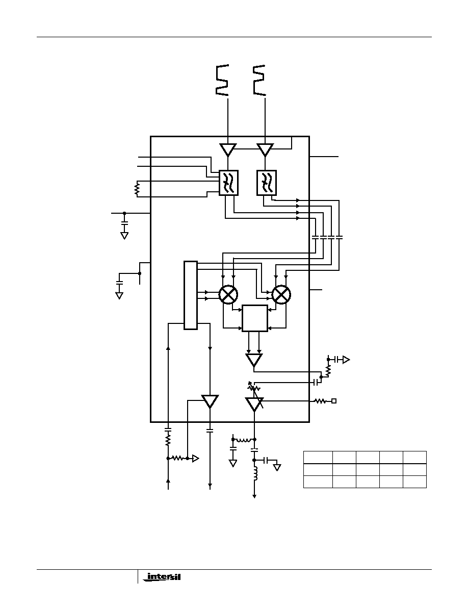
Block Diagram
0
o
/9
0
o
MOD_LO_IN
IF_OUT
MOD_LO_OUT
LPF_TUNE1
˜
2
LPF_SEL0
LPF_SEL1
LPF_TXI_IN
2V
LPF_TUNE0
I
LPF_TX_Q -
MOD TX I +
MOD TX Q -
LPF_TX_Q +
MOD TX Q +
MOD TX I -
LPF_TX_I -
LPF_TX_I +
LPF_TXQ_IN
V
CC
50
LO_GND
MOD_TX_PE
LPF_TX_PE
1.25V
(2XLO)
Q
V
CC
AGC_CTRL
50
NETWORK
10K
L
1
C
1
L
2
C
2
OUTPUT MATCH COMPONENTS TABLE
FREQ.
L
1
C
1
L
2
C
2
105MHz
270nH
12pF
82nH
15pF
280MHz
82nH
5.0pF
33nH
6.0pF
250
TX D or A
REF
NOTE: V
CC
, GND and Bypass capacitors not shown.
MOD_TX_IF_OUT
IF_AGC_IN
HFA3763

4-4
Pin Descriptions
PIN
SYMBOL
DESCRIPTION
9
LPF_V
CC
Supply pin for the Low pass filter. Use high quality decoupling capacitors right at the pin.
10
2V REF
Stable 2V reference voltage output for external applications. Loading must be higher than 10k
. A bypass
capacitor of at least 0.1
µ
F is required.
11
LPF_BYP
Internal reference bypass pin. This is the common voltage (V
CM
) used for the LPF digital thresholds. Requires
0.1
µ
F decoupling capacitor.
12
LPF_TXI_In
Low pass filter in phase (I) channel transmit input. Conventional or attenuated direct coupling is required for digital
inputs. AC couple for analog input.
13
LPF_TXQ_In
Low pass filter quadrature (Q) channel transmit input. Conventional or attenuated direct coupling is required for
digital inputs. AC couple for analog input.
14
NC
Connected internally for test purpose. Leave this pin floating.
15
NC
Connected internally for test purpose. Leave this pin floating.
16
LPF_Sel1
Digital control input pins. Selects four programmed cut off frequencies for the transmit channel. Tuning speed from
one cutoff to another is less than 1
µ
s.
SEL1
SEL0
CUTOFF FREQUENCY
SEL1
SEL0
CUTOFF FREQUENCY
LO
LO
2.2MHz
HI
LO
8.8MHz
LO
HI
4.4MHz
HI
HI
17.6MHz
17
LPF_Sel0
18
LPF_Tune1
These two pins are used to fine tune the Low pass filter cutoff frequency. A resistor connected between the two
pins (R
TUNE
) will fine tune the transmit filters. Refer to the tuning equation in the LPF AC specifications.
19
LPF_Tune0
20
TX D or A
Selects the configuration of the Transmit baseband input for either Digital or Analog (500mV
P-P
max).
Tie to a High for Analog and Ground for Digital inputs. Requires decoupling capacitor for analog and a simple direct
coupled attenuator for digital inputs.
22
LPF_TX_PE
Digital input control pin to enable the LPF transmit mode of operation. Enable logic level is High.
23
LPF_TXQ-
Negative output of the transmit Low pass filter, quadrature channel. AC coupling is required. Normally connects to
the inverting input of the quadrature Modulator (Mod_TXQ-), pin 40.
24
LPF_TXQ+
Positive output of the transmit Low pass filter, quadrature channel. AC coupling is required. Normally connects to
the non inverting input of the quadrature Modulator (Mod_TXQ+), pin 39.
25
LPF_TXI-
Negative output of the transmit Low pass filter, in phase channel. AC coupling is required. Normally connects to
the inverting input of the in phase Modulator (Mod_TXI-), pin 38.
26
LPF_TXI+
Positive output of the transmit Low pass filter, in phase channel. AC coupling is required. Normally connects to the
non inverting input of the in phase Modulator (Mod_TXI+), pin 37.
27
NC
Connected internally for test purpose. Leave this pin floating.
28
NC
Connected internally for test purpose. Leave this pin floating.
29
NC
Connected internally for test purpose. Leave this pin floating.
30
NC
Connected internally for test purpose. Leave this pin floating.
33
NC
Connected internally for test purpose. Leave this pin floating.
34
NC
Connected internally for test purpose. Leave this pin floating.
35
NC
Connected internally for test purpose. Leave this pin floating.
36
NC
Connected internally for test purpose. Leave this pin floating.
37
Mod_TXI+
In phase modulator non inverting input. AC coupling is required. This input is normally coupled to the Low pass
filter positive output (LPF_TXI+), pin 26.
38
Mod_TXI-
In phase modulator inverting input. AC coupling is required. This input is normally coupled to the Low pass filter
negative output (LPF_TXI-), pin 25.
39
Mod_TXQ+
Quadrature modulator non inverting input. AC coupling is required. This input is normally coupled to the Low pass
filter positive output (LPF_TXQ+), pin 24.
40
Mod_TXQ-
Quadrature modulator inverting input. AC coupling is required. This input is normally coupled to the Low pass filter
negative output (LPF_TXQ-), pin 23.
HFA3763
4-5
41
Mod_TX_PE
Digital input control to enable the Modulator section. Enable logic level is High for transmit.
42
Mod_TX_IF_Out
Modulator open collector output, single ended. Termination resistor to V
CC
with a typical value of 250
.
44
Mod_LO_In
(2XLO)
Single ended local oscillator current input. Frequency of input signal must be twice the required modulator carrier
LO frequency. Input current is optimum at 200
µ
A
RMS
. Input matching networks and filters can be designed for a
wide range of power and impedances at this port. Typical input impedance is 130
.
This pin requires AC coupling.
NOTE: High second harmonic content input waveforms may degrade I/Q phase accuracy.
45
Mod_V
CC
Modulator supply pin. Use high quality decoupling capacitors right at the pin.
46
Mod_LO_Out
Divide by 2 buffered output reference from "Mod_LO_in" input. Used for external applications where the
modulating and demodulating carrier reference frequency is required. 50
single end driving capability. AC
coupling is required. This output can be disabled by shorting to V
CC
or floating pin 50.
47
Mod_V
CC
Modulator supply pin. Use high quality decoupling capacitors right at the pin.
48
MOD_BYP
This pin must be connected to pin 49 and decoupled to gnd. (Note 1)
49
MOD_BYP
This pin must be connected to pin 48. (Note 1)
50
LO_GND
When grounded, this pin enables the LO buffer (Mod_LO_Out). When open (NC) it disables the LO buffer.
55
IF_AGC_IN
AC coupled input to the AGC amplifier.
57
AGC_V
CC
AGC supply pin supply pin. Use high quality decoupling capacitors right at the pin.
59
AGC_CTRL
AGC control DC control voltage input requires external resistor to set scale factor. 10K for optimum temp. co. May
require decoupling filtering capacitor.
61
AGC_V
CC
AGC supply pin supply pin. Use high quality decoupling capacitors right at the pin.
63
AGC_PE
Digital input control for the AGC amplifier. Enable logic level is High.
65
AGC_IF_OUT
AGC amplifier output. Output impedance of 250
. Need to be connected to V
CC
by an inductor with reactance
well above 250
.
67
AGC_V
CC
AGC supply pin supply pin. Use high quality decoupling capacitors right at the pin.
See
Pinout
GND
All remaining pins not listed above must be connected to a solid ground plane.
NOTE:
1. If pin 50 is grounded, otherwise float.
Pin Descriptions
(Continued)
PIN
SYMBOL
DESCRIPTION
HFA3763