 | –≠–ª–µ–∫—Ç—Ä–æ–Ω–Ω—ã–π –∫–æ–º–ø–æ–Ω–µ–Ω—Ç: HFA3767 | –°–∫–∞—á–∞—Ç—å:  PDF PDF  ZIP ZIP |
1
Æ
FN4298.3
P RE L IMIN A RY
HFA3767
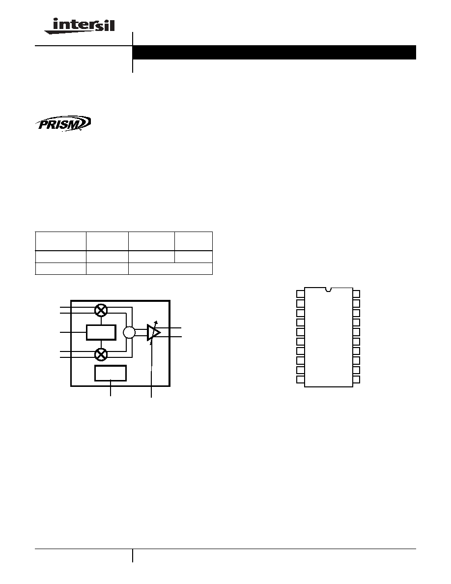
130MHz CDMA/AMPS Quadrature
Modulator and AGC
The HFA3767 is a monolithic bipolar
quadrature modulator with gain control
for CDMA/AMPS cellular applications.
An upconverter quadrature mixer and
an output gain control stage with better
than 70dB of dynamic range are integrated in the design. A
local oscillator input requires low drive levels and a divide by
two phase shifter with duty cycle compensation achieves
excellent phase and amplitude balance properties. The
HFA3767 is one of the four chips in the PRISMTM chip set
and is housed in a 20 lead SSOP package ideally suited to
cellular handset applications.
Simplified Block Diagram
Features
∑ I/Q Amplitude and Phase Balance . . . . . . . . . . . 0.5dB, 2
o
∑ 130MHz AGC Amplifier/Attenuator range . . . . . . . .>70dB
∑ Low LO Drive Level . . . . . . . . . . . . . . . . . . . . . . . .-10dBm
∑ Power Enable/Disable Control
∑ Single Supply Battery Operation . . . . . . . . . . . 2.7 to 3.3V
Applications
∑ IS95A CDMA/AMPS Dual Mode Handsets
∑ Wideband CDMA Handsets
∑ Full Duplex Transceivers
∑ CDMA/TDMA Packet Protocol Radios
∑ Portable Battery Powered Equipment
Pinout
HFA3767
(SSOP)
TOP VIEW
Ordering Information
PART NUMBER
TEMP.
RANGE (
o
C)
PACKAGE
PKG. NO.
HFA3767IA
-40 to 85
20 Ld SSOP
M20.15
HFA3767IA96
-40 to 85
Tape and Reel
˜
2 0/90
o
IF LO
TXI
TXQ
IF
OUTPUT
AGC_CTRL
BIAS
NETWORK
TX_PE
20
19
18
17
16
15
14
13
12
11
1
2
3
4
5
6
7
8
9
10
TX_PE
GND
TXI+
TXI-
NC
TXQ-
TXQ+
MIX_GND
DPS_GND
DPS_V
CC
V
CC
AGC_CTRL
GC
AGC_V
CC
TX_IF-
TX_IF+
AGC_GND
CAP
LO_IN
LO_GND
Data Sheet
February 1998
CAUTION: These devices are sensitive to electrostatic discharge; follow proper IC Handling Procedures.
1-888-INTERSIL or 321-724-7143
|
Intersil (and design) is a registered trademark of Intersil Americas Inc.
Copyright © Intersil Americas Inc. 2002. All Rights Reserved
PRISMÆ is a registered trademark of Intersil Americas Inc. PRISM and design is a trademark of Intersil Americas Inc.
2
Pin Descriptions
PIN NUMBER
NAME
DESCRIPTION
1
TX_PE
Power enable control input. HIGH for normal operation. LOW for power down.
2
GND
Bias and AGC control ground return.
3
TXI+
Positive I channel baseband input. Requires a 1.2VDC common mode bias voltage.
4
TXI-
Negative I channel baseband input. Requires a 1.2VDC common mode bias voltage.
5
NC
No connect pin. Tie to ground to improve isolation from I to Q channels.
6
TXQ-
Negative QI channel baseband input. Requires a 1.2VDC common mode bias voltage.
7
TXQ+
Positive Q channel baseband input. Requires a 1.2VDC common mode bias voltage.
8
MIX_GND
Quadrature Mixers ground return.
9
DPS_GND
Digital Phase shifter ground return.
10
DPS_V
CC
Digital Phase Shifter Power Supply. Use high quality RF decoupling capacitors right at the pin.
11
LO_GND
Local Oscillator Input ground return.
12
LO_IN
Local Oscillator Current Input. Use a 50
power to current converter.See applications diagram.
13
CAP
AGC Bias circuit filter capacitor. Typical value of 1000pF to 10000pF.
14
AGC_GND
AGC circuit ground return.
15
TX_IF+
Positive IF output port. Requires a DC return to V
CC
thru a choke or match inductor.
16
TX_IF-
Negative IF output port. Requires a DC return to V
CC
thru a choke or match inductor.
17
AGC_V
CC
AGC circuit Power Supply.Use high quality RF decoupling capacitors right at the pin.
18
GCT
Gain and temperature compensation external resistor. See applications diagram.
19
AGC_CTRL
AGC control input. Require a 1% resistor divider at this input. See applications diagram.
20
V
CC
Bias and AGC control Power Supply.Use high quality RF decoupling capacitors right at the pin.
HFA3767

3
Absolute Maximum Ratings
T
A
= 25
o
C
Thermal Information
Supply Voltage. . . . . . . . . . . . . . . . . . . . . . . . . . . . . . -0.3V to +3.6V
Voltage on Any Other Pin . . . . . . . . . . . . . . . . . -0.3V to V
CC
+0.3V
Operating Conditions
Supply Voltage Range . . . . . . . . . . . . . . . . . . . . . . . . . . 2.7V to 3.3V
Temperature Range. . . . . . . . . . . . . . . . . . . . . . .-40
o
C
T
A
85
o
C
Thermal Resistance (Typical, Note 1)
JA
(
o
C/W)
SSOP Package . . . . . . . . . . . . . . . . . . . . . . . . . . . .
115
Maximum Junction Temperature (Plastic Package) . . . . . . . . 150
o
C
Maximum Storage Temperature Range . . . . . . -65
o
C
T
A
150
o
C
Maximum Lead Temperature (Soldering 10s) . . . . . . . . . . . . . 300
o
C
(Lead Tips Only)
CAUTION: Stresses above those listed in "Absolute Maximum Ratings" may cause permanent damage to the device. This is a stress only rating and operation of the
device at these or any other conditions above those indicated in the operational sections of this specification is not implied.
NOTE:
1.
JA
is measured with the component mounted on an evaluation PC board in free air.
Electrical Specifications
V
CC
= 2.7V to 3.3V, LO_IN = -10dBM at 260MHz. Refer to Applications diagram
PARAMETER
TEST CONDITIONS
(NOTE 2)
TEST
LEVEL
TEMP
(
o
C)
MIN
TYP
MAX
UNITS
CDMA MODE SPECIFICATIONS: I AND Q INPUTS at 0.63V
PP
Sinusoidal, 500KHz in Quadrature (SSB Output)
Output Power into 50
Vagc = 0.5V , Output from
400 to 50
Differential to single end
converter
(0dB Attenuation)
A
25
-13.1
-12.7
-12.3
dBm
P1dBO/Output Power Ratio
A
Full
8
12.4
-
dB
Output Noise Floor
B
25
-
-142.3
-140
dBm/Hz
P1dBO/Output Power Ratio
AGC_CTRL set for 10dB
of attenuation
B
Full
8
12.4
-
dB
Output Noise Floor
B
25
-
-144
-
dBm/Hz
P1dBO/Output Power Ratio
AGC_CTRL set for 20dB
of attenuation
B
25
8
12.4
-
dB
Output Noise Floor
B
25
-
-148.5
-
dBm/Hz
P1dBO/Output Power Ratio
AGC_CTRL set for 30dB
of attenuation
B
25
8
12.4
-
dB
Output Noise Floor
B
25
-
-153.4
-
dBm/Hz
P1dBO/Output Power Ratio
AGC_CTRL set for 40dB
of attenuation
A
Full
8
12.4
-
dB
Output Noise Floor
B
25
-
-160
-
dBm/Hz
P1dBO/Output Power Ratio
AGC_CTRL set for 50dB
of attenuation
A
Full
8
12.4
-
dB
Output Noise Floor
B
25
-
-163
-
dBm/Hz
P1dBO/Output Power Ratio
AGC_CTRL set for 70dB
of attenuation
B
25
8
12.4
-
dB
Output Noise Floor
B
25
-
-165
-162
dBm/Hz
FM MODE SPECIFICATIONS Q INPUT ONLY at 0.44V
PP
DC Differential at Q Input. Commom Mode Voltage at I Input
Output Power into 50
Vagc = 0.5V , Output from
400 to 50
Differential to single end
converter
(0dB Attenuation)
A
Full
-10.2
-9.76
-9.3
dBm
P1dBO/Output Power Ratio
A
Full
7
10.2
-
dB
Output Noise Floor
B
25
-
-142.3
-140
dBm/Hz
GENERAL SPECIFICATIONS: I AND Q INPUTS at 0.63V
PP
Sinusoidal, 500kHz in Quadrature (SSB Output)
AGC Gain Control Voltage
A
25
0.5
-
2.4
V
AGC Gain Control Sensitivity
B
25
-
50
-
dB/V
AGC Gain Control Input Impedance
Externally set
C
25
-
18
-
k
AGC Switching Speed, Full Scale
To
±
1dB Settling
B
25
-
-
10
µ
s
HFA3767

4
AGC Insertion Phase
20dB step
B
25
-
1.6
-
deg/dB
IF Frequency Range
Applications diagram
B
25
-
130
-
MHz
GENERAL SPECIFICATIONS: I AND Q INPUTS at 0.63V
PP
Sinusoidal, 500kHz in Quadrature (SSB Output)
TX_IF Single End Equivalent Series R
130MHZ, IF+ or IF-
B
25
-
115
-
W
TX_IF Single End Equivalent Series C
130MHz, IF+ or IF-
B
25
-
4.9
-
pF
Baseband Frequency Range
B
25
DC
-
1.0
MHz
LO Frequency Range
Applications diagram
A
25
-
260
-
MHz
Amplitude Balance (Note 3)
Deviation from ideal SSB
characteristics
AGC_CTRL = 0.5V
B
25
-0.5
-
+
0.5
dB
Phase Balance (Note 3)
B
25
-2
-
+
2
Degrees
Single Sideband Suppression
A
Full
32
35
-
dBc
Carrier Suppression
(Vagc = 0.5V)
(0dB attenuation)
A
25
-30
-
-
dBc
AGC_CTRL set for 20dB
attenuation
A
25
-30
-
-
dBc
AGC_CTRL set for
70dB attenuation
B
25
-29
-
-
dBc
LO Input Impedance
Single end
C
25
-
130
-
LO Drive Level
Applications diagram
A
25
-
-10
-
dBm
LO Drive Optimal Current Range
B
25
50
200
300
µ
Arms
Baseband Differential Input Impedance
C
25
2K
-
-
VCM Common Mode Input Voltage
Into I+, I-, Q+ and Q-
A
Full
1.14
1.20
1.26
V
POWER SUPPLY AND LOGIC SPECIFICATIONS
Supply Voltage Range
B
25
2.7
-
3.3
V
Supply Current at 3.3V
AGC_CTRL = 0.5V
A
Full
-
-
40
mA
AGC_CTRL = 2.4V
A
Full
-
-
25
mA
Power Down Supply Current
TX_PE = Low
A
25
-
-
100
µ
A
Power Down Speed
B
Full
-
-
10
µ
s
TX_PE V
IL
A
Full
-
-
0.8
V
TX_PE V
IH
A
Full
2.0
-
-
V
TX_PE Input Bias Current at V
CC
= 3.3V
PE = 2.0V
A
Full
-50
-
+
50
µ
A
PE = 0.66V, 2.7V
CC
A
Full
-50
-
+
50
µ
A
NOTES:
2. A = Production Tested, B = Based on Characterization, C = By Design
3. I leading Q produces a positive frequency offset from the carrier (USB).Test garanteed by sideband suppression.
Electrical Specifications
V
CC
= 2.7V to 3.3V, LO_IN = -10dBM at 260MHz. Refer to Applications diagram (Continued)
PARAMETER
TEST CONDITIONS
(NOTE 2)
TEST
LEVEL
TEMP
(
o
C)
MIN
TYP
MAX
UNITS
HFA3767
5
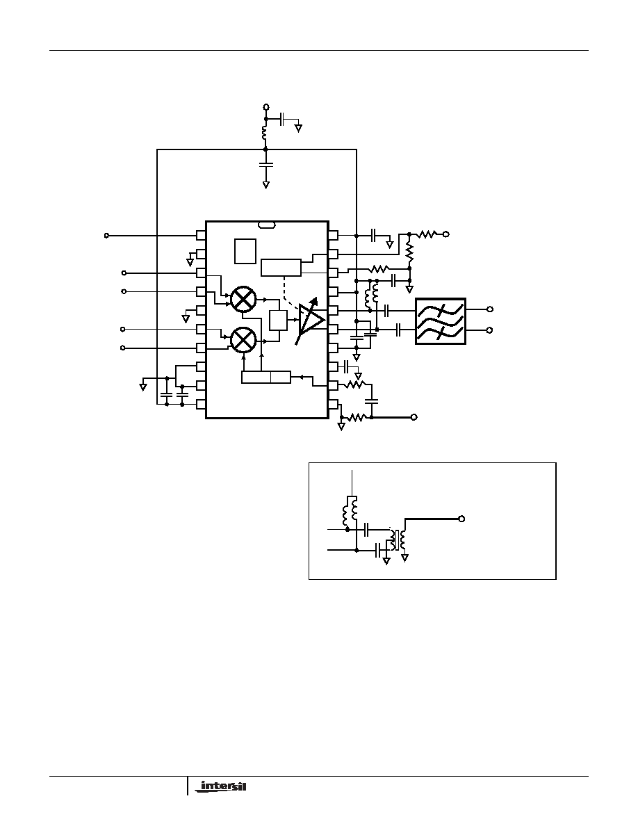
Applications Diagram
0
o
/90
o
LO_IN
˜
2
LO_GND
TX_PE
NC
GND
TXI+
TXI-
TXQ+
TXQ-
MIX_GND
DPS_GND
DPS_V
CC
CAP
AGC_GND
TX_IF-
TX_IF+
AGC_V
CC
GC
V
CC
BIAS
AGC_CTRL
.1
BEAD
1
0.03
100p
0.03
1000p
0.03
100p
220
1000p
56
LO_IN
MINI CIRCUITS. TC8-1
3.6k 1%
3.6k 1%
I+
I-
Q+
Q-
V
CC
AGC_CTRL
15K 1%
POWER ENABLE
IF+
IF-
220n
220n
4p
4p
50
OUTPUT
V
CC
TX_IF+
TX_IF-
DIFFERENTIAL TO 50
SINGLE END
CONVERTER (1.1dB INSERTION LOSS)
.01
0.01
TEST OUTPUT NETWORK
1
80n
1
80n
4.7p
4.7p
MURATA
LFSH33
CONTROL
HFA3767