 | –≠–ª–µ–∫—Ç—Ä–æ–Ω–Ω—ã–π –∫–æ–º–ø–æ–Ω–µ–Ω—Ç: HFA3783IN | –°–∫–∞—á–∞—Ç—å:  PDF PDF  ZIP ZIP |
TM
1
File Number
4633.2
HFA3783
I/Q Modulator/Demodulator and
Synthesizer
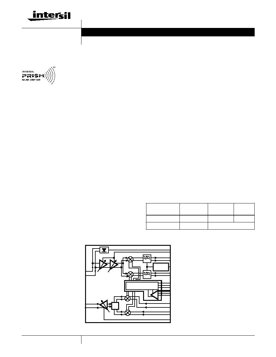
The HFA3783 is a highly integrated and
fully differential SiGe baseband
converter for half duplex wireless
applications. It features all the
necessary blocks for quadrature
modulation and demodulation of "I" and "Q" baseband
signals.
It has an integrated AGC receive IF amplifier with frequency
response to 600MHz. The AGC has 70dB of voltage gain
and better than 70dB of gain control range. The transmit
output also features gain control with 70dB of range.
The receive and transmit IF paths can share a common
differential matching network to reduce the filter component
count required for single IF half duplex transceivers. A pair of
2nd order antialiasing filters with an integrated DC offset
cancellation architecture is included in the receive chain for
baseband operation down to DC. In addition, an IF level
detector is included in the AGC chain for threshold
comparison. Up and down conversion are performed by
doubly balanced mixers for "I" and "Q" IF processing. These
converters are driven by a broadband quadrature LO
generator with frequency of operation phase locked by an
internal 3 wire interface synthesizer and PLL.
The device operates at low LO levels from an external VCO
with a PLL reference signal up to 50MHz. The HFA3783 is
housed in a thin 48 lead LQFP package well suited for
PCMCIA board applications.
Features
∑ Integrates All IF Transmit and Receive Functions
∑ Broad Quadrature Frequency Range . . . . . .70 to 600MHz
∑ 600MHz AGC IF Strip with Level Detector . . . . . . . . .69dB
∑ DC Coupled Baseband Interfaces
∑ Integrates a Receiver DC Offset Calibration Loop
∑ Integrated 3 Wire Interface PLL For LO Applications
∑ Low LO Drive Level . . . . . . . . . . . . . . . . . . . . . . . -15dBm
∑ Fast Transmit-Receive Switching . . . . . . . . . . . . . . . . <1
µ
s
∑ Power Management/Standby Mode
∑ Single Supply 2.7 to 3.3V Operation
Applications
∑ IEEE802.11 1 and 2Mbps Standard
∑ Systems Targeting IEEE 802.11 11Mbps Standard
∑ Wireless Local Area Networks
∑ PCMCIA Wireless Transceivers
∑ ISM Systems
∑ TDMA Packet Protocol Radios
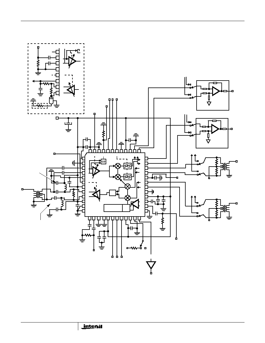
Simplified Block Diagram
Ordering Information
PART
NUMBER
TEMP. RANGE
(
o
C)
PACKAGE
PKG. NO.
HFA3783IN
-40 to 85
48 Ld LQFP
Q48.7x7A
HFA3783IN96
-40 to 85
Tape and Reel
0
o
/90
o
PLL MODULE
REF IN
IF 2X LO / VCO IN
3 WIRE INTERFACE
BASEBAND TX I
BASEBAND TXQ
TRANSMIT IF AGC
BASEBAND RXI
BASEBAND RXQ
RECEIVE AGC
IF DETECTOR OUT
CHARGE PUMP OUT
IF_IN
IF_OUT
OFFSET
CAL
CAL ENABLE
I
Q
Data Sheet
March 2000
CAUTION: These devices are sensitive to electrostatic discharge; follow proper IC Handling Procedures.
1-888-INTERSIL or 321-724-7143
|
Intersil and Design is a trademark of Intersil Corporation.
|
Copyright
©
Intersil Corporation 2000
PRISM is a registered trademark of Intersil Corporation. PRISM logo is a trademark of Intersil Corporation.
2
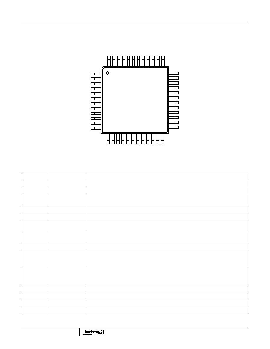
Pinout
Pin Descriptions
PIN NUMBER
NAME
DESCRIPTION
1
RX_V
CC
Receive AGC Amplifier Power Supply. Requires high quality capacitor decoupling.
3
IF_RX+
Receive AGC Differential Amplifier Non-Inverting IF Input. Requires a DC blocking capacitor.
4
IF_RX-
Receive AGC Differential Amplifier Inverting IF Input. Requires a DC blocking capacitor. Pins 3 and 4 are
interchangeable and can be used single ended with the other being capacitively bypassed to ground.
6
TX_VAGC
Transmit AGC amplifier DC gain control input.
7
TX_V
CC
Transmit AGC Amplifier Power Supply. Requires high quality capacitor decoupling.
8
IF_TX+
Transmit AGC Differential Amplifier Positive Output. Open collector requiring DC bias from V
CC
through
an inductor.
9
IF_TX-
Transmit AGC Differential Amplifier Negative Output. Open collector requiring DC bias from V
CC
through
an inductor.
10
TX_V
CC
Transmit AGC Amplifier Power Supply. Requires high quality capacitor decoupling.
13
REF_BYP
PLL Reference Buffer Signal Negative Differential Input. Pin has active bias and can be used in
conjunction with pin 14 either differential or single ended. CMOS inputs must be DC coupled. Small
sinusoidal inputs must be DC blocked with this pin bypassed to ground via a capacitor.
14
REF_IN
PLL Reference Buffer Signal Positive Differential Input. Pin has active bias and can be used in conjunction
with pin 13 either differential or single ended. CMOS inputs must be DC coupled. Small sinusoidal inputs
must be DC blocked with this pin used as an input for the reference signal. When used with single ended
CMOS inputs, pin 13 must be left floating. Pins 13 and 14 are interchangeable.
17
SYN_V
DD
PLL Synthesizer Digital Power Supply. Requires high quality capacitor decoupling.
18
CLK
PLL Synthesizer Serial Interface Clock. CMOS input.
19
DATA
PLL Synthesizer Serial Interface Data. CMOS input.
20
LE
PLL Synthesizer Serial Interface Latch Enable Control. CMOS input.
1
2
3
4
5
6
7
8
32
31
30
29
28
27
26
25
24
23
22
21
20
19
18
17
9
10
11
12
13 14 15 16
33
34
35
36
37
38
39
40
41
42
43
44
45
46
47
48
RXQ+
RXQ-
TXI+
TXI-
1.2V_OUT
TXQ+
TXQ-
GND
LO_V
CC
LO_IN+
LO_IN-
GND
RX_V
CC
GND
IF_RX+
IR_RX-
GND
IF_TX+
IF_TX-
TX_V
CC
GND
GND
TX_VAGC
TX_V
CC
GND
RX_V
A
G
C
GND
IF_DET
PE1
CAL_EN
GND
BB_V
CC
GND
RXI+
RXI-
PE2
REF_BYP
REF_IN
GND
GND
SYN_V
DD
CLK
DA
T
A
LE
CP_V
DD
CP_D0
GND
LD
HFA3783
3
21
CP_V
DD
PLL Charge Pump Power Supply. Independent supply for the charge pump, not to exceed 3.6V. Requires
high quality capacitor decoupling.
22
CP_D0
PLL Charge Pump Current Output.
24
LD
PLL Lock Detect Output. Requires low capacitive loading not to exceed 5pF.
26
LO_IN-
Local Oscillator Differential Buffer Negative Input. Requires AC coupling. For single ended applications
its complementary input, Pin 27, must be bypassed to ground via a capacitor.
27
LO_IN+
Local Oscillator Differential Buffer Positive Input. Requires AC coupling. For single ended applications its
complementary input, Pin 26, must be bypassed to ground via a capacitor. Pins 26 and 27 are
interchangeable.
NOTE: High second harmonic content LO waveforms may degrade I/Q phase accuracy.
28
LO_V
CC
Local Oscillator Buffer Amplifier Power Supply. Requires high quality capacitor decoupling.
30
TXQ-
Baseband Quadrature Differential Inputs for IF Transmission. DC coupled requiring 1.3V common mode
bias voltages.
31
TXQ+
32
1.2V_OUT
Highly Regulated Band Gap 1.2V Buffered Output. Used in conjunction with ADCs and DACs for voltage
/temperature tracking. Requires high quality 0.1
µ
F capacitor decoupling to ground.
33
TXI-
Baseband In Phase Differential Inputs for IF Transmission. DC coupled requiring 1.3V common mode
bias voltages.
34
TXI+
35
RXQ-
Baseband Quadrature Differential Outputs From IF Demodulation. DC coupled output with 1.2V common
mode DC outputs. AC coupling pins 35, 36, 37 and 38 requires programmable register activation for DC
hold during TX to RX switching.
36
RXQ+
37
RXI-
Baseband In Phase Differential Outputs From IF Demodulation. DC coupled output with 1.2V common
mode DC outputs.
38
RXI+
40
BB_V
CC
Baseband Receive LPF Output and Offset Control Power Supply. Requires high quality capacitor
decoupling.
42
CAL_EN
CMOS Input for Activation Of Internal DC Offset Adjust Circuit for the Receive Baseband Outputs. A rising
edge activates the calibration cycle, which completes within a programmable time and holds the
calibration while this pin is held high. In applications where the synthesizer is not used, this pin needs to
be grounded.
43
PE2
Power Enable Control Pins: Please refer to the POWER ENABLE TRUTH TABLE in the Electrical
Specifications section.
44
PE1
45
IF_DET
IF Detector Current Output. A current source of 175
µ
A typical is generated at this pin when the IF AGC
receive differential or single ended signal at pins 3 and 4 is between 100 and 200mV
PP
.
47
RX_VAGC
Receive AGC amplifier DC gain control input.
2, 5, 11, 12, 15,
16, 23, 25, 29,
39, 41, 46, 48
GND
Grounds. Connect to a solid ground plane.
Pin Descriptions
(Continued)
PIN NUMBER
NAME
DESCRIPTION
HFA3783
4
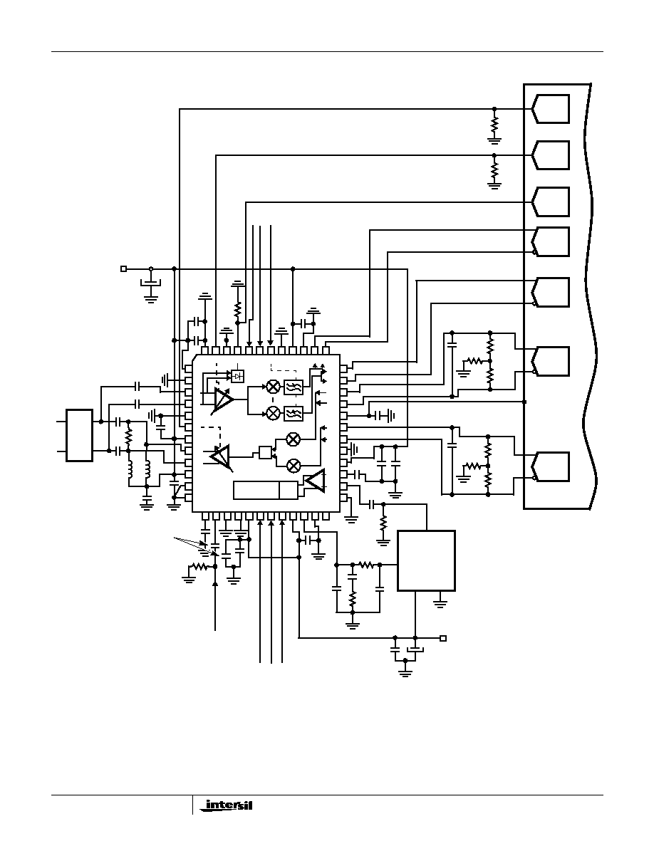
Application Circuit
100p
21 22 23 24
25
26
27
28
29
30
31
32
33
34
35
36
1
2
3
4
5
6
7
8
9
10
11
12
13 14 15 16
48 47 46 45
37
38
39
40
44 43 42 41
17 18 19 20
0/90
SYNTH
2K
100p
100p
1000p
1000p
49.9
1000p
0.01
0.1
0.022
0.22
2K
3.92K
100p
0.1
0.1
0.01
100p
2.87K
L
P
L
P
C
S
C
S
VT
0.1
56
0.01
56p
124
124
536
124
124
536
619
976
IDAC
7 BITS
TX_VAGC
IDAC
7 BITS
RX_VAGC
1-BIT
IF_DET
ADC
6 BITS
RX"I"
ADC
6 BITS
RX"Q"
DAC
6 BITS
TX"I"
TX"Q"
1.2V REF IN
HFA3861
FROM MAC (CAL+ EN CTRL)
VCO_V
CC
VCO
PANASONIC
ENFV25F80
RF
FROM MAC (PLL CTRL)
REF FREQ
(SINUSOIDAL)
10
µ
0.1
10
µ
V
CC
LO
SAW
DET
DAC
6 BITS
1000p
3900pF
68p
68p
SAWTEK
855653L1
HFA3783
5
Test Diagram
21 22 23 24
25
26
27
28
29
30
31
32
33
34
35
36
1
2
3
4
5
6
7
8
9
10
11
12
13 14 15 16
48 47 46 45
37
38
39
40
44 43 42 41
17 18 19 20
100p
100p
270p
1000p
1000p
.01
.1
100p
100p
.1
.1
.01
2.87K
.1
50
.01
270p
56p
(SINUSOIDAL)
10
µ
V
CC
LO
COMMON MODE VOLTAGE
CALIBRATION
CALIBRATION
1.2V REF.
CALIBRATION
CALIBRATION
TC4-1W
2K
8p
8p
27n
27n
1000p
MATCH COMPONENTS FOR
IF IN/OUT
REF_IN
50
CLK
DA
T
A
LE
VCC/2
CP
(LOW INPUT CAPACITANCE)
LO_IN (2X FREQ)
1.2V_OUT
RX_VAGC
IF_DET
PE1
PE2
CAL_EN
TXQ
V
CC
50
50
1000p
1000p
FREQUENCY RESPONSE TEST SET UP
50
200p
50
ANALYZER
SWEEP
9
8
7
5
4
3
2
6
GEN.
0/90
SYNTH
5K
INPUT
RXI
5K
INPUT
RXQ
COMMON MODE VOLTAGE
TXI
BUFFER
TEST FIXTURE (374MHz)
AND TRANSFORMER
TX_VAGC
100p
1000p
HFA3783