2-99
HFA3824A
Direct Sequence Spread Spectrum
Baseband Processor
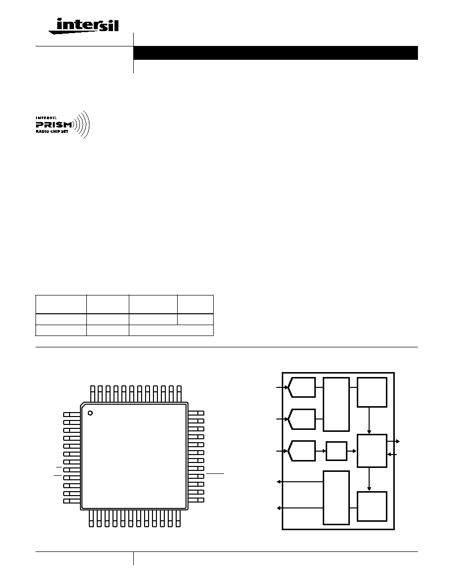
The Intersil HFA3824A Direct
Sequence (DSSS) baseband
processor is part of the PRISMTM
2.4GHz radio chipset, and contains all
the functions necessary for a full or
half duplex packet baseband transceiver.
The HFA3824A has on-board ADC's for analog I and Q
inputs, for which the HFA3724/6 IF QMODEM is
recommended. Differential phase shift keying modulation
schemes DBPSK and DQPSK, with optional data scrambling
capability, are combined with a programmable PN sequence
of up to 16 bits. Built-in flexibility allows the HFA3824A to be
configured through a general purpose control bus, for a wide
range of applications. A Receive Signal Strength Indicator
(RSSI) monitoring function with on-board 6-bit 2 MSPS ADC
provides Clear Channel Assessment (CCA) to avoid data
collisions and optimize network throughput. The HFA3824A
is housed in a thin plastic quad flat package (TQFP) suitable
for PCMCIA board applications.
Features
∑ Complete DSSS Baseband Processor
∑ High Data Rate. . . . . . . . . . . . . . . . . . . . . . .up to 4 MBPS
∑ Processing Gain . . . . . . . . . . . . . . . . . . . . . . . . up to 12dB
∑ Programmable PN Code . . . . . . . . . . . . . . . . up to 16 Bits
∑ Ultra Small Package . . . . . . . . . . . . . . . . . . . . 7 x 7 x 1mm
∑ Single Supply Operation (44MHz Max) . . . . . 2.7V to 5.5V
∑ Modulation Method. . . . . . . . . . . . . . . . DBPSK or DQPSK
∑ Supports Full or Half Duplex Operations
∑ On-Chip A/D Converters for I/Q Data (3-Bit, 44 MSPS)
and RSSI (6-Bit, 2 MSPS)
∑ Backward Compatible with HSP3824
∑ Programmable Rotation I, Q Sense
Applications
∑ Systems Targeting IEEE802.11 Standard
∑ DSSS PCMCIA Wireless Transceiver
∑ Spread Spectrum WLAN RF Modems
∑ TDMA Packet Protocol Radios
∑ Part 15 Compliant Radio Links
∑ Portable Bar Code Scanners/POS Terminal
∑ Portable PDA/Notebook Computer
∑ Wireless Digital Audio
∑ Wireless Digital Video
∑ PCN/Wireless PBX
Ordering Information
PART NO.
TEMP.
RANGE (
o
C)
PKG. TYPE
PKG. NO.
HFA3824AIV
-40 to 85
48 Ld TQFP
Q48.7x7
HFA3824AIV96
-40 to 85
Tape and Reel
TM
Pinout
HFA3824A (TQFP)
Simplified Block Diagram
1
2
3
4
5
6
7
8
32
31
30
29
28
27
26
25
24
23
22
21
20
19
18
17
9
10
11
12
13 14 15 16
33
34
35
36
37
38
39
40
41
42
43
44
45
46
47
48
RXCLK
RXD
MD_RDY
RX_PE
CCA
GND
MCLK
V
DD
RESET
ANTSEL
A/D_CAL
SD
TEST_CK
TX_PE
TXD
TXCLK
TX_RDY
R/W
CS
V
DDA
GND
I
IN
GND
V
DD
I
OUT
Q
OUT
TEST7
TEST6
TEST5
V
DD
GND
TEST3
TEST2
TEST1
TEST0
TEST4
Q
IN
RSSI
GND
V
REFP
V
REFN
V
DD
A
GND
V
DD
A
V
DD
GND
AS
SCLK
RSSI
I
IN
Q
IN
I
OUT
Q
OUT
DPSK
DEMOD.
PRO-
CESSOR
DPSK
MOD.
D
A
T
A
T
O
NETW
ORK
CTRL
PR
OCESSOR
6-BIT
A/D
3-BIT
A/D
3-BIT
A/D
CCA
SPREADER
DE-SPREADER
INTER-
FACE
Data Sheet
August 1998
File Number
4459.2
CAUTION: These devices are sensitive to electrostatic discharge; follow proper IC Handling Procedures.
http://www.intersil.com or 407-727-9207
|
Copyright
©
Intersil Corporation 1999
PRISMÆ is a registered trademark of Intersil Corporation. PRISM logo is a trademark of Intersil Corporation.

2-100
Table of Contents
PAGE
Ordering Information . . . . . . . . . . . . . . . . . . . . . . . . . . . . . . . . . . . . . . . . . . . . . . . . . . . . . . . . . . . . . . . . . . . . . . . . . . . . . . . . 2-99
Pinout . . . . . . . . . . . . . . . . . . . . . . . . . . . . . . . . . . . . . . . . . . . . . . . . . . . . . . . . . . . . . . . . . . . . . . . . . . . . . . . . . . . . . . . . . . . . 2-99
Simplified Block Diagram . . . . . . . . . . . . . . . . . . . . . . . . . . . . . . . . . . . . . . . . . . . . . . . . . . . . . . . . . . . . . . . . . . . . . . . . . . . . . 2-99
Typical Application Diagram. . . . . . . . . . . . . . . . . . . . . . . . . . . . . . . . . . . . . . . . . . . . . . . . . . . . . . . . . . . . . . . . . . . . . . . . . . . 2-101
Pin Description . . . . . . . . . . . . . . . . . . . . . . . . . . . . . . . . . . . . . . . . . . . . . . . . . . . . . . . . . . . . . . . . . . . . . . . . . . . . . . . . . . . . . 2-102
External Interfaces . . . . . . . . . . . . . . . . . . . . . . . . . . . . . . . . . . . . . . . . . . . . . . . . . . . . . . . . . . . . . . . . . . . . . . . . . . . . . . . . . . 2-105
Control Port . . . . . . . . . . . . . . . . . . . . . . . . . . . . . . . . . . . . . . . . . . . . . . . . . . . . . . . . . . . . . . . . . . . . . . . . . . . . . . . . . . . . . . . 2-105
TX Port . . . . . . . . . . . . . . . . . . . . . . . . . . . . . . . . . . . . . . . . . . . . . . . . . . . . . . . . . . . . . . . . . . . . . . . . . . . . . . . . . . . . . . . . . . . 2-108
RX Port. . . . . . . . . . . . . . . . . . . . . . . . . . . . . . . . . . . . . . . . . . . . . . . . . . . . . . . . . . . . . . . . . . . . . . . . . . . . . . . . . . . . . . . . . . . 2-109
I/Q ADC Interface . . . . . . . . . . . . . . . . . . . . . . . . . . . . . . . . . . . . . . . . . . . . . . . . . . . . . . . . . . . . . . . . . . . . . . . . . . . . . . . . . . . 2-109
ADC Calibration Circuit and Registers . . . . . . . . . . . . . . . . . . . . . . . . . . . . . . . . . . . . . . . . . . . . . . . . . . . . . . . . . . . . . . . . . . . 2-110
RSSI ADC Interface . . . . . . . . . . . . . . . . . . . . . . . . . . . . . . . . . . . . . . . . . . . . . . . . . . . . . . . . . . . . . . . . . . . . . . . . . . . . . . . . . 2-110
Test Port. . . . . . . . . . . . . . . . . . . . . . . . . . . . . . . . . . . . . . . . . . . . . . . . . . . . . . . . . . . . . . . . . . . . . . . . . . . . . . . . . . . . . . . . . . 2-110
Definitions. . . . . . . . . . . . . . . . . . . . . . . . . . . . . . . . . . . . . . . . . . . . . . . . . . . . . . . . . . . . . . . . . . . . . . . . . . . . . . . . . . . . . . . . . 2-111
External AGC Control. . . . . . . . . . . . . . . . . . . . . . . . . . . . . . . . . . . . . . . . . . . . . . . . . . . . . . . . . . . . . . . . . . . . . . . . . . . . . . . . 2-111
Power Down Modes . . . . . . . . . . . . . . . . . . . . . . . . . . . . . . . . . . . . . . . . . . . . . . . . . . . . . . . . . . . . . . . . . . . . . . . . . . . . . . . . . 2-111
Reset . . . . . . . . . . . . . . . . . . . . . . . . . . . . . . . . . . . . . . . . . . . . . . . . . . . . . . . . . . . . . . . . . . . . . . . . . . . . . . . . . . . . . . . . . . . . 2-112
Transmitter Description . . . . . . . . . . . . . . . . . . . . . . . . . . . . . . . . . . . . . . . . . . . . . . . . . . . . . . . . . . . . . . . . . . . . . . . . . . . . . . 2-112
Header/Packet Description. . . . . . . . . . . . . . . . . . . . . . . . . . . . . . . . . . . . . . . . . . . . . . . . . . . . . . . . . . . . . . . . . . . . . . . . . . . . 2-113
PN Generator Description . . . . . . . . . . . . . . . . . . . . . . . . . . . . . . . . . . . . . . . . . . . . . . . . . . . . . . . . . . . . . . . . . . . . . . . . . . . . . 2-114
Scrambler and Data Encoder Description . . . . . . . . . . . . . . . . . . . . . . . . . . . . . . . . . . . . . . . . . . . . . . . . . . . . . . . . . . . . . . . . 2-115
Modulator Description . . . . . . . . . . . . . . . . . . . . . . . . . . . . . . . . . . . . . . . . . . . . . . . . . . . . . . . . . . . . . . . . . . . . . . . . . . . . . . . 2-116
Clear Channel Assessment (CCA) and Energy Detect (ED) Description. . . . . . . . . . . . . . . . . . . . . . . . . . . . . . . . . . . . . . . . . 2-116
Receiver Description . . . . . . . . . . . . . . . . . . . . . . . . . . . . . . . . . . . . . . . . . . . . . . . . . . . . . . . . . . . . . . . . . . . . . . . . . . . . . . . . 2-116
Acquisition Description . . . . . . . . . . . . . . . . . . . . . . . . . . . . . . . . . . . . . . . . . . . . . . . . . . . . . . . . . . . . . . . . . . . . . . . . . . . . . . . 2-117
Two Antenna Acquisition . . . . . . . . . . . . . . . . . . . . . . . . . . . . . . . . . . . . . . . . . . . . . . . . . . . . . . . . . . . . . . . . . . . . . . . . . . . 2-117
One Antenna Acquisition . . . . . . . . . . . . . . . . . . . . . . . . . . . . . . . . . . . . . . . . . . . . . . . . . . . . . . . . . . . . . . . . . . . . . . . . . . . 2-117
Acquisition Signal Quality Parameters . . . . . . . . . . . . . . . . . . . . . . . . . . . . . . . . . . . . . . . . . . . . . . . . . . . . . . . . . . . . . . . . . 2-117
Procedure to Set Acq. Signal Quality Parameters (Example) . . . . . . . . . . . . . . . . . . . . . . . . . . . . . . . . . . . . . . . . . . . . . . . 2-118
PN Correlator Description . . . . . . . . . . . . . . . . . . . . . . . . . . . . . . . . . . . . . . . . . . . . . . . . . . . . . . . . . . . . . . . . . . . . . . . . . . . . 2-119
Data Demodulation and Tracking Description . . . . . . . . . . . . . . . . . . . . . . . . . . . . . . . . . . . . . . . . . . . . . . . . . . . . . . . . . . . . . 2-119
Procedure to Set Signal Quality Registers . . . . . . . . . . . . . . . . . . . . . . . . . . . . . . . . . . . . . . . . . . . . . . . . . . . . . . . . . . . . . . 2-119
Data Decoder and Descrambler Description. . . . . . . . . . . . . . . . . . . . . . . . . . . . . . . . . . . . . . . . . . . . . . . . . . . . . . . . . . . . . . . . 2-120
Demodulator Performance . . . . . . . . . . . . . . . . . . . . . . . . . . . . . . . . . . . . . . . . . . . . . . . . . . . . . . . . . . . . . . . . . . . . . . . . . . . . 2-120
Overall Eb/N0 Versus BER Performance . . . . . . . . . . . . . . . . . . . . . . . . . . . . . . . . . . . . . . . . . . . . . . . . . . . . . . . . . . . . . . . 2-120
Clock Offset Tracking Performance . . . . . . . . . . . . . . . . . . . . . . . . . . . . . . . . . . . . . . . . . . . . . . . . . . . . . . . . . . . . . . . . . . . 2-121
Carrier Offset Frequency Performance. . . . . . . . . . . . . . . . . . . . . . . . . . . . . . . . . . . . . . . . . . . . . . . . . . . . . . . . . . . . . . . . . 2-121
I/Q Amplitude Imbalance . . . . . . . . . . . . . . . . . . . . . . . . . . . . . . . . . . . . . . . . . . . . . . . . . . . . . . . . . . . . . . . . . . . . . . . . . . . 2-121
A Default Register Configuration . . . . . . . . . . . . . . . . . . . . . . . . . . . . . . . . . . . . . . . . . . . . . . . . . . . . . . . . . . . . . . . . . . . . . . . 2-121
Control Registers . . . . . . . . . . . . . . . . . . . . . . . . . . . . . . . . . . . . . . . . . . . . . . . . . . . . . . . . . . . . . . . . . . . . . . . . . . . . . . . . . . . 2-124
Waveforms . . . . . . . . . . . . . . . . . . . . . . . . . . . . . . . . . . . . . . . . . . . . . . . . . . . . . . . . . . . . . . . . . . . . . . . . . . . . . . . . . . . . . . . . 2-137
HFA3824A

2-101
Typical Application Diagram
For additional information on the PRISMTM chip set, call
(407) 724-7800 to access Intersil' AnswerFAX system. When
prompted, key in the four-digit document number (File #) of
the data sheets you wish to receive.
The four-digit file numbers are shown in Typical Application
Diagram, and correspond to the appropriate circuit.
QUAD IF MODULATOR
RFPA
HFA3925
HFA3724/6
DSSS BASEBAND PROCESSOR
D
A
T
A
T
O
MA
C
CTRL
HFA3824, HFA3824A
TUNE/SELECT
HFA3524
0
o
/90
o
VCO
A/D
A/D
MAC-PHY
INTERFACE
802.11
VCO
DUAL SYNTHESIZER
HFA3624
UP/DOWN
CONVERTER
A/D
(FILE# 4067)
(FILE# 4308, 4459)
(FILE# 4062)
(FILE# 4066)
(FILE# 4132)
PRISMTM CHIP SET FILE #4063
M
U
X
M
U
X
DPSK
DEMOD
DPSK
MOD.
DE-
SPREAD
SPREAD
Q
I
HFA3424
(NOTE)
(FILE# 4131)
TYPICAL TRANSCEIVER APPLICATION CIRCUIT USING THE HFA3824A
NOTE: Required for systems targeting 802.11 specifications.
CCA
RXI
RXQ
RSSI
TXI
TXQ
˜
2
HFA3824A
2-102
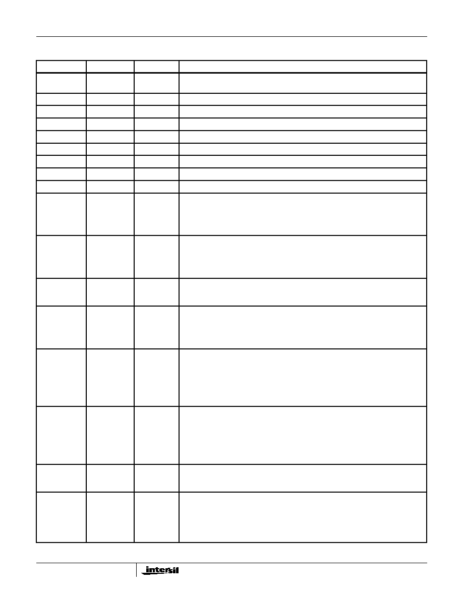
Pin Description
NAME
PIN
TYPE I/O
DESCRIPTION
V
DDA
(Analog)
10, 18, 20
Power
DC power supply 2.7V - 5.5V (Not Hardwire Together On Chip).
V
DD
(Digital)
7, 21, 29, 42
Power
DC power supply 2.7V - 5.5V
GND (Analog)
11, 15, 19
Ground
DC power supply 2.7V - 5.5V, ground (Not Hardwire Together On Chip).
GND (Digital)
6, 22, 31, 41
Ground
DC power supply 2.7V - 5.5V, ground.
V
REFN
17
I
"Negative" voltage reference for ADC's (I and Q) [Relative to V
REFP
]
V
REFP
16
I
"Positive" voltage reference for ADC's (I, Q and RSSI)
I
IN
12
I
Analog input to the internal 3-bit A/D of the In-phase received data.
Q
IN
13
I
Analog input to the internal 3-bit A/D of the Quadrature received data.
RSSI
14
I
Receive Signal Strength Indicator Analog input.
A/D_CAL
26
O
This signal is used internally as part of the I and Q ADC calibration circuit. When the ADC
calibration circuit is active, the voltage references of the ADCs are adjusted to maintain the
outputs of the ADCs in their optimum range. A logic 1 on this pin indicates that one or both
of the ADC outputs are at their full scale value. This signal can be integrated externally as
a control voltage for an external AGC.
TX_PE
2
I
When active, the transmitter is configured to be operational, otherwise the transmitter is in
standby mode. TX_PE is an input from the external Media Access Controller (MAC) or net-
work processor to the HFA3824A. The rising edge of TX_PE will start the internal transmit
state machine and the falling edge will inhibit the state machine. TX_PE envelopes the
transmit data.
TXD
3
I
TXD is an input, used to transfer serial Data or Preamble/Header information bits from the
MAC or network processor to the HFA3824A. The data is received serially with the LSB
first. The data is clocked in the HFA3824A at the falling edge of TXCLK.
TXCLK
4
O
TXCLK is a clock output used to receive the data on the TXD from the MAC or network
processor to the HFA3824A, synchronously. Transmit data on the TXD bus is clocked into
the HFA3824A on the falling edge. The clocking edge is also programmable to be on either
phase of the clock. The rate of the clock will be depending upon the modulation type and
data rate that is programmed in the signalling field of the header.
TX_RDY
5
O
When the HFA3824A is configured to generate the preamble and Header information in-
ternally, TX_RDY is an output to the external network processor indicating that Preamble
and Header information has been generated and that the HFA3824A is ready to receive
the data packet from the network processor over the TXD serial bus. The TX_RDY returns
to the inactive state when the TX_PE goes inactive indicating the end of the data transmis-
sion. TX_RDY is an active high signal. This signal is meaningful only when the HFA3824A
generates its own preamble.
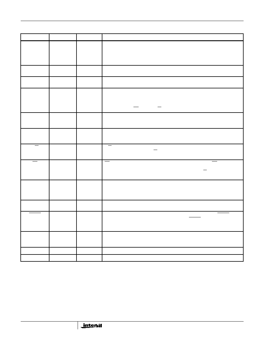
CCA
32
O
Clear Channel Assessment (CCA) is an output used to signal that the channel is clear to
transmit. The CCA algorithm is user programmable and makes its decision as a function
of RSSI, Energy detect (ED), and Carrier Sense (CRS). The CCA algorithm and its pro-
grammable features are described in the data sheet.
Logic 0 = Channel is clear to transmit.
Logic 1 = Channel is NOT clear to transmit (busy).
This polarity is programmable and can be inverted.
RXD
35
O
RXD is an output to the external network processor transferring demodulated Header in-
formation and data in a serial format. The data is sent serially with the LSB first. The data
is frame aligned with MD_RDY.
RXCLK
36
O
RXCLK is the clock output bit clock. This clock is used to transfer Header information and
data through the RXD serial bus to the network processor. This clock reflects the bit rate
in use. RXCLK will be held to a logic "0" state during the acquisition process. RXCLK be-
comes active when the HFA3824A enters in the data mode. This occurs once bit sync is
declared and a valid signal quality estimate is made, when comparing the programmed sig-
nal quality thresholds.
HFA3824A
2-103
MD_RDY
34
O
MD_RDY is an output signal to the network processor, indicating a data packet is ready to
be transferred to the processor. MD_RDY is an active high signal and it envelopes the data
transfer over the RXD serial bus. MD_RDY returns to its inactive state when there is no
more receiver data, when the programmable data length counter reaches its value or when
the link has been interrupted. MD_RDY remains inactive during preamble synchronization.
RX_PE
33
I
When active, receiver is configured to be operational, otherwise receiver is in standby
mode. This is an active high input signal. In standby, all A/D converters are disabled.
ANTSEL
27
O
The antenna select signal changes state as the receiver switches from antenna to antenna
during the acquisition process in the antenna diversity mode.
SD
25
I/O
SD is a serial bidirectional data bus which is used to transfer address and data to/from the
internal registers. The bit ordering of an 8-bit word is MSB first. The first 8 bits during trans-
fers indicate the register address immediately followed by 8 more bits representing the
data that needs to be written or read at that register. This pin goes to high impedance
(three-state) when CS is high or R/W is low.
SCLK
24
I
SCLK is the clock for the SD serial bus. The data on SD is clocked at the rising edge. SCLK
is an input clock and it is asynchronous to the internal master clock (MCLK)The maximum
rate of this clock is 11MHz or one half the master clock frequency, whichever is lower.
AS
23
I
AS is an address strobe used to envelope the Address or the data on SD.
Logic 1 = envelopes the address bits.
Logic 0 = envelopes the data bits.
R/W
8
I
R/W is an input to the HFA3824A used to change the direction of the SD bus when reading
or writing data on the SD bus. R/W must be set up prior to the rising edge of SCLK. A high
level indicates read while a low level is a write.
CS
9
I
CS is a Chip select for the device to activate the serial control port. The CS doesn't impact
any of the other interface ports and signals, i.e., the TX or RX ports and interface signals.
This is an active low signal. When inactive SD, SCLK, AS and R/W become "don't care"
signals.
TEST 0-7
37, 38, 39, 40,
43, 44, 45, 46
I/O
This is a data port that can be programmed to bring out internal signals or data for moni-
toring. These bits are primarily reserved by the manufacturer for testing. A further descrip-
tion of the test port is given at the appropriate section of this data sheet. The direction of
these pins are not established until programming of test registers is complete.
TEST_CK
1
O
This is the clock that is used in conjunction with the data that is being output from the test
bus (TEST 0-7).
RESET
28
I
Master reset for device. When active TX and RX functions are disabled. If RESET is kept
low the HFA3824A goes into the power standby mode. RESET does not alter any of the
configuration register values nor it presets any of the registers into default values. Device
requires programming upon power-up.
MCLK
30
I
Master Clock for device. The maximum frequency of this clock is 44MHz. This is used in-
ternally to generate all other internal necessary clocks and is divided by 1, 2, 4, or 8 for the
transceiver clocks.
I
OUT
48
O
TX Spread baseband I digital output data. Data is output at the programmed chip rate.
Q
OUT
47
O
TX Spread baseband Q digital output data. Data is output at the programmed chip rate.
NOTE: Total of 48 pins; ALL pins are used.
Pin Description
(Continued)
NAME
PIN
TYPE I/O
DESCRIPTION
HFA3824A