1
TM
File Number
8020
CAUTION: These devices are sensitive to electrostatic discharge; follow proper IC Handling Procedures.
1-888-INTERSIL or 321-724-7143
|
Intersil and Design is a trademark of Intersil Americas Inc.
Copyright © Intersil Americas Inc. 2001, All Rights Reserved
P RE L I M I N A RY
HFA3842B
PCMCIA/USB Wireless LAN Medium
Access Controller
The Intersil HFA3842B Wireless LAN
Medium Access Controller is part of
the PRISMÆ 2.4GHz radio chip set.
The HFA3842B directly interfaces
with the Intersil HFA386x family of Baseband Processors,
offering a complete end-to-end chip set solution for wireless
LAN products. Protocol and PHY support are implemented in
firmware to allow custom protocol and different PHY
transceivers.
The HFA3842B is designed to provide maximum
performance with minimum power consumption. Package
pin layout provides optimal PC board layout to all user
interfaces including PCMCIA and USB.
Firmware implements the full IEEE 802.11 Wireless LAN
MAC protocol. It supports BSS and IBSS operation under
DCF, and operation under the optional Point Coordination
Function (PCF). Low level protocol functions such as
RTS/CTS generation and acknowledgement, fragmentation
and de-fragmentation, and automatic beacon monitoring are
handed without host intervention. Active scanning is
performed autonomously once initiated by host command.
Host interface command and status handshakes allow
concurrent operations from multi-threaded I/O drivers.
Additional firmware functions specific to access point
applications are also available.
Designing wireless protocol systems using the HFA3842B is
made easier with the availability of evaluation board, firm-
ware, software device drivers, and complete documentation.
The HFA3842B is a WLAN MAC Controller IC, based on the
HFA3841. Pin-for-pin upgrade replacement for the HFA3841.
Applications
∑ High Data Rate Wireless LAN
∑ PC Card Wireless LAN Adapters
∑ USB Wireless LAN Adapters
∑ PCI Wireless LAN Cards (Using Ext. Bridge Chip)
∑ Wireless LAN Modules
∑ Wireless LAN Access Points
∑ Wireless Bridge Products
∑ Wireless Point-to-Multipoint Systems
∑ ISA, ISA PNP WLAN Cards
Features
∑ USB Host Interface supports USB V1.1 at 12Mbps, and is
an alternative to the PC Card host interface.
∑ New start up modes allow the PCMCIA Card Information
Structure to be initialized from a serial EEPROM. This
allows firmware to be downloaded from the host,
eliminating the parallel Flash memory device.
∑ Firmware can be loaded from serial Flash memory.
∑ Direct attachment to a typical x16 SRAM using five control
signals (RAMCS_, MOE_, MWEL_, MLBE_, and MUBE_).
∑ Low frequency crystal oscillator to maintain time and allow
baseband clock source to power off during sleep mode.
∑ Improved performance of internal WEP engine.
∑ On-chip execution can now be viewed while in debug
mode.
∑ Independent programmable cycle timing for external chip
selects allows attachment of slow memory devices without
compromising higher speed instruction execution.
∑ Pinout is backward compatible with HFA3841.
∑ IEEE802.11 Standard Data Rates: 1, 2, 5.5 and 11Mbps
∑ Part of the Intersil PRISM Wireless LAN Chip Set
∑ Full Implementation of the MAC Protocol Specified in IEEE
Standards 802.11-1999 and 802.11b
∑ PCMCIA Host Interface Supports Full 16-Bit
Implementation of PC Card 16 (1995), also ISA PNP with
Additional Chip
∑ Host Interface Provides Dual Buffer Access Paths
∑ External Memory Interface Supports up to 4M bytes RAM
∑ Internal Encryption Engine Executes IEEE802.11 WEP
∑ Low Power Operation; 25mA Active, 8mA Doze, <1mA
Sleep
∑ Operation at 2.7V to 3.6V Supply
∑ 5V Tolerant Host Interface Input/Outputs
∑ 128 Pin LQFP Package Targeted for Type II PC Cards
∑ IEEE802.11 Wireless LAN MAC Protocol Firmware and
MicrosoftÆ WindowsÆ Software Drivers
∑ Pin for Pin Replacement for the HFA3841 Supporting all
Functions and operations of the HFA3841
Ordering Information
PART
NUMBER
TEMP. RANGE
(
o
C)
PACKAGE
PKG. NO.
HFA3842BIN
-40 to 85
128 Ld LQFP
Q128.14x20
HFA3842BIN-TK
-40 to 85
Tape and Reel
Data Sheet
June 2001
MicrosoftÆ and WindowsÆ are registered trademarks of Microsoft Corporation.
PRISMÆ is a registered trademark of Intersil Americas Inc.
PRISM and design is a trademark of Intersil Americas Inc.
2
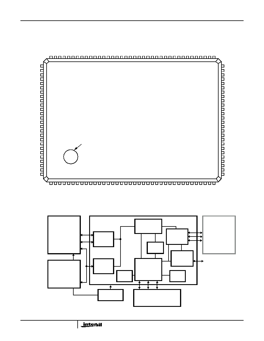
Pinout
128 LEAD LQFP
Simplified Block Diagram
103
66
64
63
62
61
60
59
58
57
56
55
54
53
52
51
50
49
48
47
46
45
44
43
42
41
40
MA
8
MA
7
MA
6
MA
5
MA
3
MA
2
MA
4
MA
9
MA
17
MA
16
MA
15
MA
14
MA
12
MA
1
1
MA
10
V
CC
_IO
3
V
SS
_IO
3
MA
13
MA
18
HD8
HD9
HD1
0
PL
7
MO
E
-
RAM
CS
-
NV
CS
-
V
CC
_IO
3
PJ
4
V
SS
_IO
3
MW
E
L
-
MA
1
MA
0/M
W
E
H
-
PJ
2
PJ
1
PJ
3
PK
7
PK
6
V
SS
_C
O
R
E
3
V
CC
_C
O
R
E
3
PL
2
PL
1
PL
3
PJ
0
PL
0
V
CC
_C
O
R
E
3
V
SS
_C
O
R
E
3
US
B+
TC
LK
I
N
R
E
SET
TX
D
TX
C
RX
D
RX
C
PJ
7
HD6
HD7
HCE
1
-
HD5
HD4
HD3
PJ
6
PJ
5
US
B-
V
SS
_IO
3
V
CC
_IO
3
HD2
HD1
HD0
HRE
G
-
PK
5
72
73
74
75
76
77
67
68
69
70
71
83
84
85
86
78
79
80
81
82
92
93
94
95
96
97
87
88
89
90
91
98
INDEX
1
3
4
5
6
7
8
9
10
11
12
13
14
15
16
17
18
19
20
21
22
23
24
25
26
27
28
29
30
31
32
PK
2
PK
1
PK
0
HS
T
S
CHG
-
V
SS
_C
O
R
E
3
CL
KO
UT
LFXTALI
CLKIN
LFXTALO
V
SS
_IO3
PL4
MD15
MD14
MD13
MD12
MD11
MD10
MD9
MD8
V
SS
_IO3
V
CC
_CORE3
MD7
MD6
MD5
MD4
MD3
MD2
MD1
MD0
MLBE-
PK3
PK4
2
33
34
35
36
37
38
99
10
0
10
1
1
0
2
104
105
106
107
108
109
110
111
112
113
114
115
116
117
118
119
120
121
122
123
124
125
126
127
128
HINPACK-
HWAIT-
HA0
HA1
HA2
HA3
HA4
HA5
HA6
HA7
HIREQ-
V
SS
_IO3
HWE-
HA8
HA9
HIOWR-
HIORD-
HOE-
HCE2-
HD15
V
CC
_IO3
HD14
HD13
HD12
HD11
SB ATTACHED
39
65
PRISM RADIO
TXD/RXD
CTRL/STATUS
SERIAL CONTROL
PHY
SERIAL
CONTROL
(MMI)
PRISM RADIO
RADIO AND SYNTH
MICRO-
PROGRAMMED
MAC ENGINE
MEMORY
WEP
ENGINE
PC CARD
ON-CHIP
RAM
44MHz CLOCK
SOURCE
DA
T
A
AD
DR
E
S
S
SE
L
E
C
T
EXTERNAL
SRAM AND
FLASH
MEMORY
HOST
COMPUTER
DATA
ADDRESS
HFA3842B
USB
HOST
INTERFACE
USB
CONTROL
ON-CHIP
ROM
BASEBAND
PROCESSOR
RF SECTION
SERIAL CONTROL
INTERFACE
(MDI)
CONTROLLER
HOST
INTERFACE
THE 3842 MUST BE SUPPLIED WITH A
SEPARATE 48MHz CLOCK WHEN USB IS USED.
HFA3842B
3
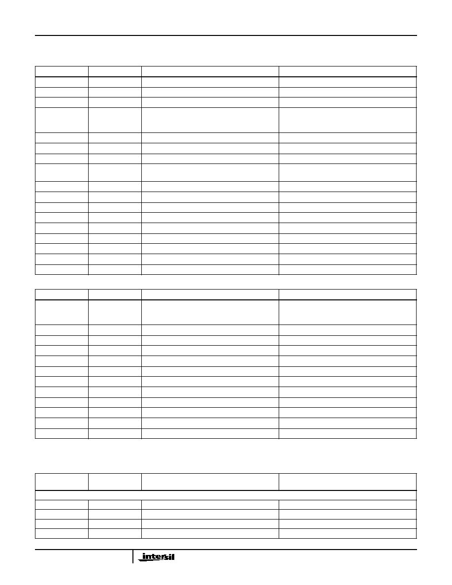
HFA3842B Pin Descriptions
HOST INTERFACE PINS
PIN NAME
PIN NUMBER
PIN I/O TYPE
DESCRIPTION
HA0-9
106-113, 117, 118 5V Tol, CMOS, Input, 50K Pull Down
PC Card Address Input, Bits 0 to 9
HCE1-
1
5V Tol, CMOS, Input, 50K Pull Up
PC Card Select, Low Byte
HCE2-
122
5V Tol, CMOS, Input, 50K Pull Up
PC Card Select, High Byte
HD0-15
101-99, 6-2,
96-94, 128-125,
123
5V Tol, BiDir, 2mA, 50K Pull Down
PC Card Data Bus, Bit 0 to 15
HINPACK-
103
CMOS Output, 2mA
PC Card I/O Decode Confirmation
HIORD-
120
5V Tol, CMOS, Input, 50K Pull Up
PC Card I/O Space Read
HIOWR-
119
5V Tol, CMOS, Input, 50K Pull Up
PC Card I/O Space Write
HRDY/HIREQ-
114
CMOS Output, 4mA
PC Card interrupt Request (I/O Mode) Card Ready
(Memory Mode)
HOE-
121
5V Tol, CMOS, Input, 50K Pull Up
PC Card Memory Attribute Space Output Enable
HREG-
102
5V Tol, CMOS, Input, 50K Pull Up
PC Card Attribute Space Select
HRESET
16
5V Tol, CMOS, ST Input, 50K Pull Up
Hardware Reset
HSTSCHG-
36
CMOS Output, 4mA
PC Card Status Change
HWAIT-
104
CMOS Output, 4mA
PC Card Not Ready (Force Host Wait State)
HWE-
116
5V Tol, CMOS Input, 50K Pull Up
PC Card Memory Attribute Space Write Enable
USB+
12
CMOS BiDir, 2mA, (Also USB Transceiver)
USB, MBUS Address Bit 20, or I/O as PL5
USB-
11
CMOS BiDir, 2mA, (Also USB Transceiver)
USB, MBUS Address Bit 21, or I/O or I/O as PL6
USB ATTACHED
105
Input, 5V Tolerant, Pull-Down
Sense USB VBUS to Indicate Cable Attachment
TABLE 1. MEMORY INTERFACE PINS
PIN NAME
PIN NUMBER
PIN I/O TYPE
DESCRIPTION
MUBE- / MA0 /
MWEH-
72
CMOS TS Output, 2mA
MBUS Upper Byte Enable for x16 Memory; MBUS
Address Bit 0 (byte) for x8 Memory; High Byte Write
Enable for 2 x8 Memories
MA1-18
73-81, 84-92
CMOS TS Output, 2mA
MBUS Address Bits 1 to 18
PL4
43
CMOS BiDir, 2mA
MBUS Address Bit 19
PL5
12
CMOS BiDir, 2mA, 50K Pull Up
MBUS Address Bit 20 (See Note 1)
PL6
11
CMOS BiDir, 2mA
MBUS Address Bit 21 (See Note 1)
MLBE-
62
CMOS TS Output, 2mA, 50K Pull Up
MBUS Lower Byte Enable, or I/O as PM2
MOE-
70
CMOS TS Output, 2mA
Memory Output Enable
MWE- / MWEL-
71
CMOS TS Output, 2mA
Low (or only) Byte Memory Write Enable
RAMCS-
69
CMOS TS Output, 2mA
RAM Select
NVCS-
68
CMOS TS Output, 2mA
NV Memory Select
MD0-7
61-54
5V Tol, CMOS, BiDir, 2mA, 100K Pull Up
MBUS Low Data Byte, Bits 0 to 7
MD8-15
51-44
5V Tol, CMOS, BiDir, 2mA 50K Pull Down
MBUS High Data Byte, Bits 8 to 15
NOTE:
1. Not available if USB interface is used.
TABLE 2. GENERAL PURPOSE AND EEPROM PORT PINS
PIN NAME
PIN NUMBER
PIN I/O TYPE
DESCRIPTION OF FUNCTION
(IF OTHER THAN IO PORT)
GENERAL PURPOSE PORT PINS
TXD
17
CMOS BiDir, 2mA, 50K Pull Down
Transmit Data Out
TXC
18
CMOS BiDir, 2mA
Transmit Clock In/Out
RXD
19
CMOS Input
Receive Data In
RXC
20
CMOS Input
Receive Clock In
HFA3842B
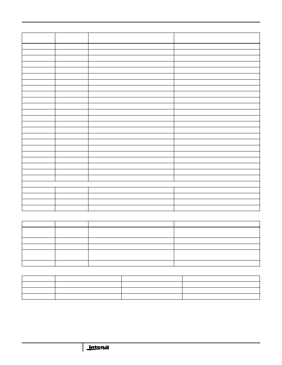
4
PJ0
31
CMOS BiDir, 2mA, 50K Pull Down
MMI Clock (SCLK)
PJ1
32
CMOS BiDir, 2mA, 50K Pull Down
MMI Serial Data (SD)
PJ3
29
CMOS BiDir, 2mA
MMI Device Enable 0 (CS_BAR)
PJ4
65
CMOS BiDir, 2mA
MMI Device Enable 1 (PE1)
PJ5
8
CMOS BiDir, 2mA, 50K Pull Up
MBUS Request (LE_IF)
PJ6
7
CMOS BiDir, 2mA
MBUS Grant; LED
PJ7
9
CMOS BiDir, 2mA, 50K Pull Up
(RADIO_PE)
PK0
35
CMOS BiDir, 2mA, ST, 50K Pull Down
MPSI Clock (LE_RF)
PK1
34
CMOS BiDir, 2mA, 50K Pull Down
MPSI Data Out (SYNTHCLK)
PK2
33
CMOS BiDir, 2mA, 50K Pull Down
MPSI Data In (SYNTHDATA)
PK3
63
CMOS BiDir, 2mA
MPSI Device Select 0 (PA_PE)
PK4
64
CMOS BiDir, 2mA
MPSI Device Select 1 (PE2)
PK5
21
CMOS BiDir, 2mA
PHY Data Available (MDREADY)
PK6
22
CMOS BiDir, 2mA
PHY Medium Busy (CCA)
PK7
23
CMOS BiDir, 2mA
PHY Energy Detect (CAL_EN)
PL0
15
CMOS BiDir, 2mA
Transmitter Enable (TX_PE)
PL1
27
CMOS BiDir, 2mA
Receiver Enable (or PHY Sleep Control) (RX_PE)
PL2
26
CMOS BiDir, 2mA
PHY Reset (RESET_BB)
PL3
28
CMOS BiDir, 2mA
Antenna Select (T/R_SW_BAR)
PL4
43
CMOS BiDir, 2mA
MBUS Address Bit 19 (MA19)
PL5 (USB+)
12
CMOS BiDir, 2mA, (Also USB Transceiver)
MBUS Address Bit 20 (USB+)
PL6 (USB-)
11
CMOS BiDir, 2mA, (Also USB Transceiver)
MBUS Address Bit 21 (USB-)
PL7
93
CMOS BiDir, 2mA, Pull Down
PHY Transmit Ready (T/R_SW)
SERIAL EEPROM PORT PINS
PJ0
31
CMOS BiDir
SCLK, Serial Clock
PJ1
30
CMOS BiDir, 50K Pull Down
SD, Serial Data Out
PJ2
32
CMOS BiDir, 50K Pull Down
MISO, Serial Data IN
TCLKIN (CS_)
10
CMOS BiDir
CS_, Chip Select
TABLE 3. CLOCKS
PIN NAME
PIN NUMBER
PIN I/O TYPE
DESCRIPTION
CLKIN
40
CMOS Input, ST Pull Down
External Clock Input (at >= 2X Desired MCLK
Frequency, Typically 44-48MHz)
LFXTALI
39
Analog Input
32.768kHz Crystal Input (Note 2)
LFXTALO
41
CMOS Output, 2mA
32.768kHz Crystal Output
CLKOUT
38
CMOS, TS Output, 2mA
Clock Output (Selectable as MCLK, TCLK, or
TOUT0)
TCLKIN
10
CMOS BiDir, 2mA, 50K Pull Down
Alternate clock input for timers
TABLE 4. POWER
PIN NAME
PIN NUMBER
PIN I/O TYPE
DESCRIPTION
V
CC
14, 25, 53, 66, 83, 98, 124
3.3V Supply
V
CC
_IO5
105
5V Tolerance Supply
V
SS
13, 24, 37, 42, 52, 67, 82, 97, 115
GND
ST = Schmitt Trigger (Hysteresis), TS = Three-State. Signals ending with "-" are active low.
NOTE:
2. Pin 39 (V
CC
_CORE3 in 3841), has been reassigned as LFXTALI. For 3841 compatibility, it may be tied to V
CC
.
Pin 62 (TRST- in 3841) has been reassigned as MLBE. For 3841 compatibility, it may be tied low through 1K.
Pin 105 (V
CC
_IO5 in 3841) has been reassigned as USB ATTACHED. For 3841 compatibility, it may be tied to V
CC
.
Output pins typically drive to positive voltage rail less 0.1V. Hence with a supply of 2.7V the output will just meet 5V TTL signal levels at
rated loads.
TABLE 2. GENERAL PURPOSE AND EEPROM PORT PINS (Continued)
PIN NAME
PIN NUMBER
PIN I/O TYPE
DESCRIPTION OF FUNCTION
(IF OTHER THAN IO PORT)
HFA3842B
5
TABLE 5. PORT PIN USES FOR PRISM APPLICATION
PIN
NAME
PRISM I USE
PRISM II USE
20
RXC
RXC - Receive Clock
RXC - Receive Clock
19
RXD
RXD - Receive Data
RXD - Receive Data
18
TXC
TXC - Transmit Clock
TXC - Transmit Clock
17
TXD
TXD - Transmit Data
TXD - Transmit Data
31
PJ0
SCLK - Clock for the SD Serial Bus
SCLK - Clock for the SD Serial Bus
30
PJ1
SD - Serial Bidirectional Data Bus
SD - Serial Bi-Directional Data Bus
32
PJ2
R/W - An input to the HFA3860A Used to Change
the Direction of the SD Bus When Reading or
Writing Data on the SD Bus
Not Used
29
PJ3
CS - A Chip Select for the Device to Activate the
Serial Control Port (Active Low)
CS_BAR - Chip Select for HFA3861 Baseband
(Active Low)
65
PJ4
Not Used
PE1 - Power Enable 1
8
PJ5
SYNTH_LE - Latches a Frame of 22 Bits After it has
Been Shifted by the SCLK into the Synthesizer
Registers
LE_IF - Load Enable for HFA3783 Quad IF
7
PJ6
LED - Activity Indicator
LED - Activity Indicator
9
PJ7
Not Used
RADIO_PE - RF Power Enable
35
PK0
Not Used
LE_RF - Load Enable for HFA3683 RF Chip
34
PK1
Not Used
SYNTHCLK - Serial Clock to Front End Chips
33
PK2
Not Used
SYNTHDATA - Serial Data to Front End Chips
63
PK3
TX_PE_RF - Power Enable
PA_PE - Transmit PA Power Enable
64
PK4
RX_PE_RF - Power Enable
PE2 - Power Enable 2
21
PK5
MD_RDY - Header Data and Data Packet are
Ready to be Transferred From Baseband on RXD
MDREADY - Header Data and Data Packet are
Ready to be Transferred from Baseband on RXD
22
PK6
CCA - Signal that the Channel is Clear to Transmit
CCA - Signal that the Channel is Clear to Transmit
23
PK7
RADIO_PE - Master Power Control for the RF
Section
CAL_EN - Calibration Mode Enable
15
PL0
TX_PE and PA_PE - Transmit Enable to Baseband TX_PE - Transmit Enable to Baseband
27
PL1
RX_PE - Receive Enable to Baseband
RX_PE - Receive Enable to Baseband
26
PL2
RESET - Reset to Baseband
RESET_BB - Reset Baseband
28
PL3
Not Used
T/R-SW_BAR - Transient/Receive Control (Inverted)
43
PL4
MA19 (If Required)
MA19 (If Required)
12
PL5
MA20 (If Required)
MA20 (If Required) or USB+
11
PL6
MA21 (If Required)
MA21 (If Required) or USB-
93
PL7
TX_RDY - Baseband Ready to Receive Data on
TXD (Not Used By Firmware)
T/R_SW - Transmit/Receive Control
HFA3842B