2-131
HFA3860A
Direct Sequence Spread Spectrum
Baseband
The Intersil HFA3860A Direct
Sequence Spread Spectrum (DSSS)
baseband processor is part of the
PRISMTM 2.4GHz radio chipset, and
contains all the functions necessary for
a full or half duplex packet baseband transceiver.
The HFA3860A has on-board A/Ds for analog I and Q inputs,
for which the HFA3724/6 IF QMODEM is recommended.
Differential phase shift keying modulation schemes DBPSK
and DQPSK, with data scrambling capability, are available
along with M-Ary Bi-Orthogonal Keying to provide a variety
of data rates. Built-in flexibility allows the HFA3860A to be
configured through a general purpose control bus, for a
range of applications. A Receive Signal Strength Indicator
(RSSI) monitoring function with on-board 6-bit A/D provides
Clear Channel Assessment (CCA) to avoid data collisions
and optimize network throughput. The HFA3860A is housed
in a thin plastic quad flat package (TQFP) suitable for
PCMCIA board applications.
Features
∑ Complete DSSS Baseband Processor
∑ Processing Gain . . . . . . . . . . . . . . . . . . . . . . . . . .
10.4dB
∑ Programmable Data Rate. . . . . . . .1, 2, 5.5, and 11MBPS
∑ Ultra Small Package . . . . . . . . . . . . . . . . . . . . 7 x 7 x 1mm
∑ Single Supply Operation (44MHz Max) . . . . . 2.7V to 3.6V
∑ Modulation Methods . . . . . . .DBPSK, DQPSK, and MBOK
∑ Supports Full or Half Duplex Operations
∑ On-Chip A/D Converters for I/Q Data (3-Bit, 22MSPS) and
RSSI (6-Bit)
∑ Backwards Compatible with HFA3860
∑ Supports Antenna Diversity
Applications
∑ Enterprise WLAN Systems
∑ Systems Targeting Ethernet Data Rates
∑ DSSS PCMCIA Wireless Transceiver
∑ Spread Spectrum WLAN RF Modems
∑ TDMA Packet Protocol Radios
∑ Part 15 Compliant Radio Links
∑ Portable Bar Code Scanners/POS Terminal
∑ Portable PDA/Notebook Computer
∑ Wireless Digital Audio
∑ Wireless Digital Video
∑ PCN/Wireless PBX
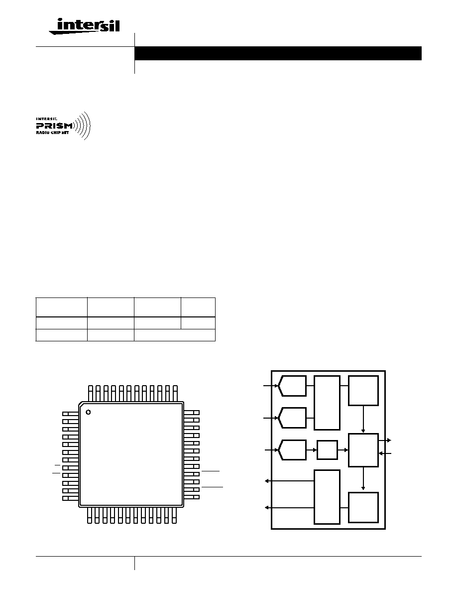
Pinout
Ordering Information
PART NO.
TEMP.
RANGE (
o
C)
PKG. TYPE
PKG. NO.
HFA3860AIV
-40 to 85
48 Ld TQFP
Q48.7x7
HFA3860AIV96
-40 to 85
Tape and Reel
TM
HFA3860A (TQFP)
SIMPLIFIED BLOCK DIAGRAM
1
2
3
4
5
6
7
8
32
31
30
29
28
27
26
25
24
23
22
21
20
19
18
17
9
10
11
12
13 14 15 16
33
34
35
36
37
38
39
40
41
42
43
44
45
46
47
48
RXCLK
RXD
MD_RDY
RX_PE
CCA
GND
MCLK
V
DD
RESET
ANTSEL
ANTSEL
SD
TEST_CK
TX_PE
TXD
TXCLK
TX_RDY
R/W
CS
V
DDA
GND
I
IN
GND
V
DD
I
OUT
Q
OUT
TEST7
TEST6
TEST5
V
DD
GND
TEST3
TEST2
TEST1
TEST0
TEST4
Q
IN
RSSI
GND
V
REFP
V
REFN
V
DD
A
GND
V
DD
A
V
DD
GND
SDI
SCLK
RSSI
I
IN
Q
IN
I
OUT
Q
OUT
DEMOD.
PRO-
CESSOR
MOD.
D
A
T
A
T
O
NETW
ORK
CTRL
PR
OCESSOR
6-BIT
A/D
3-BIT
A/D
3-BIT
A/D
CCA
SPREADER
DE-SPREADER
INTER-
FACE
Data Sheet
November 1998
File Number
4488.2
CAUTION: These devices are sensitive to electrostatic discharge; follow proper IC Handling Procedures.
http://www.intersil.com or 407-727-9207
|
Copyright
©
Intersil Corporation 1999
PRISMÆ is a registered trademark of Intersil Corporation. PRISM logo is a trademark of Intersil Corporation.

2-132
Table of Contents
PAGE
Pinout . . . . . . . . . . . . . . . . . . . . . . . . . . . . . . . . . . . . . . . . . . . . . . . . . . . . . . . . . . . . . . . . . . . . . . . . . . . . . . . . . . . . . . . . . . . . 2-131
Table of Contents . . . . . . . . . . . . . . . . . . . . . . . . . . . . . . . . . . . . . . . . . . . . . . . . . . . . . . . . . . . . . . . . . . . . . . . . . . . . . . . . . . . 2-132
Typical Application Diagram. . . . . . . . . . . . . . . . . . . . . . . . . . . . . . . . . . . . . . . . . . . . . . . . . . . . . . . . . . . . . . . . . . . . . . . . . . . 2-133
Pin Descriptions . . . . . . . . . . . . . . . . . . . . . . . . . . . . . . . . . . . . . . . . . . . . . . . . . . . . . . . . . . . . . . . . . . . . . . . . . . . . . . . . . . . . 2-133
External Interfaces . . . . . . . . . . . . . . . . . . . . . . . . . . . . . . . . . . . . . . . . . . . . . . . . . . . . . . . . . . . . . . . . . . . . . . . . . . . . . . . . . . 2-135
Control Port (4 Wire) . . . . . . . . . . . . . . . . . . . . . . . . . . . . . . . . . . . . . . . . . . . . . . . . . . . . . . . . . . . . . . . . . . . . . . . . . . . . . . . . 2-135
TX Port . . . . . . . . . . . . . . . . . . . . . . . . . . . . . . . . . . . . . . . . . . . . . . . . . . . . . . . . . . . . . . . . . . . . . . . . . . . . . . . . . . . . . . . . . . . 2-137
RX Port. . . . . . . . . . . . . . . . . . . . . . . . . . . . . . . . . . . . . . . . . . . . . . . . . . . . . . . . . . . . . . . . . . . . . . . . . . . . . . . . . . . . . . . . . . . 2-137
I/Q A/D Interface. . . . . . . . . . . . . . . . . . . . . . . . . . . . . . . . . . . . . . . . . . . . . . . . . . . . . . . . . . . . . . . . . . . . . . . . . . . . . . . . . . . . 2-138
A/D Calibration Circuit and Registers. . . . . . . . . . . . . . . . . . . . . . . . . . . . . . . . . . . . . . . . . . . . . . . . . . . . . . . . . . . . . . . . . . . . 2-139
RSSI A/D Interface . . . . . . . . . . . . . . . . . . . . . . . . . . . . . . . . . . . . . . . . . . . . . . . . . . . . . . . . . . . . . . . . . . . . . . . . . . . . . . . . . . 2-139
Test Port. . . . . . . . . . . . . . . . . . . . . . . . . . . . . . . . . . . . . . . . . . . . . . . . . . . . . . . . . . . . . . . . . . . . . . . . . . . . . . . . . . . . . . . . . . 2-140
Definitions. . . . . . . . . . . . . . . . . . . . . . . . . . . . . . . . . . . . . . . . . . . . . . . . . . . . . . . . . . . . . . . . . . . . . . . . . . . . . . . . . . . . . . . . . 2-140
Power Down Modes . . . . . . . . . . . . . . . . . . . . . . . . . . . . . . . . . . . . . . . . . . . . . . . . . . . . . . . . . . . . . . . . . . . . . . . . . . . . . . . . . 2-141
Transmitter Description . . . . . . . . . . . . . . . . . . . . . . . . . . . . . . . . . . . . . . . . . . . . . . . . . . . . . . . . . . . . . . . . . . . . . . . . . . . . . . 2-141
Header/Packet Description. . . . . . . . . . . . . . . . . . . . . . . . . . . . . . . . . . . . . . . . . . . . . . . . . . . . . . . . . . . . . . . . . . . . . . . . . . . . 2-142
Scrambler and Data Encoder Description . . . . . . . . . . . . . . . . . . . . . . . . . . . . . . . . . . . . . . . . . . . . . . . . . . . . . . . . . . . . . . . . 2-143
Spread Spectrum Modulator Description . . . . . . . . . . . . . . . . . . . . . . . . . . . . . . . . . . . . . . . . . . . . . . . . . . . . . . . . . . . . . . . . . . . 2-144
Clear Channel Assessment (CCA) and Energy Detect (ED) Description. . . . . . . . . . . . . . . . . . . . . . . . . . . . . . . . . . . . . . . . . 2-144
Demodulator Description . . . . . . . . . . . . . . . . . . . . . . . . . . . . . . . . . . . . . . . . . . . . . . . . . . . . . . . . . . . . . . . . . . . . . . . . . . . . . 2-145
Acquisition Description . . . . . . . . . . . . . . . . . . . . . . . . . . . . . . . . . . . . . . . . . . . . . . . . . . . . . . . . . . . . . . . . . . . . . . . . . . . . . . . 2-146
PN Correlators Description. . . . . . . . . . . . . . . . . . . . . . . . . . . . . . . . . . . . . . . . . . . . . . . . . . . . . . . . . . . . . . . . . . . . . . . . . . . . 2-147
Data Demodulation and Tracking Description (DBPSK and DQPSK Modes) . . . . . . . . . . . . . . . . . . . . . . . . . . . . . . . . . . . . . 2-148
Data Decoder and Descrambler Description . . . . . . . . . . . . . . . . . . . . . . . . . . . . . . . . . . . . . . . . . . . . . . . . . . . . . . . . . . . . . . . . . . . . 2-148
Data Demodulation and Tracking Description (BMBOK and QMBOK Modes) . . . . . . . . . . . . . . . . . . . . . . . . . . . . . . . . . . . . 2-148
Demodulator Performance . . . . . . . . . . . . . . . . . . . . . . . . . . . . . . . . . . . . . . . . . . . . . . . . . . . . . . . . . . . . . . . . . . . . . . . . . . . . 2-153
A Default Register Configuration . . . . . . . . . . . . . . . . . . . . . . . . . . . . . . . . . . . . . . . . . . . . . . . . . . . . . . . . . . . . . . . . . . . . . . . 2-153
Control Registers . . . . . . . . . . . . . . . . . . . . . . . . . . . . . . . . . . . . . . . . . . . . . . . . . . . . . . . . . . . . . . . . . . . . . . . . . . . . . . . . . . . 2-155
Test Circuit . . . . . . . . . . . . . . . . . . . . . . . . . . . . . . . . . . . . . . . . . . . . . . . . . . . . . . . . . . . . . . . . . . . . . . . . . . . . . . . . . . . . . . . . 2-166
HFA3860A

2-133
HFA3860A
2-134
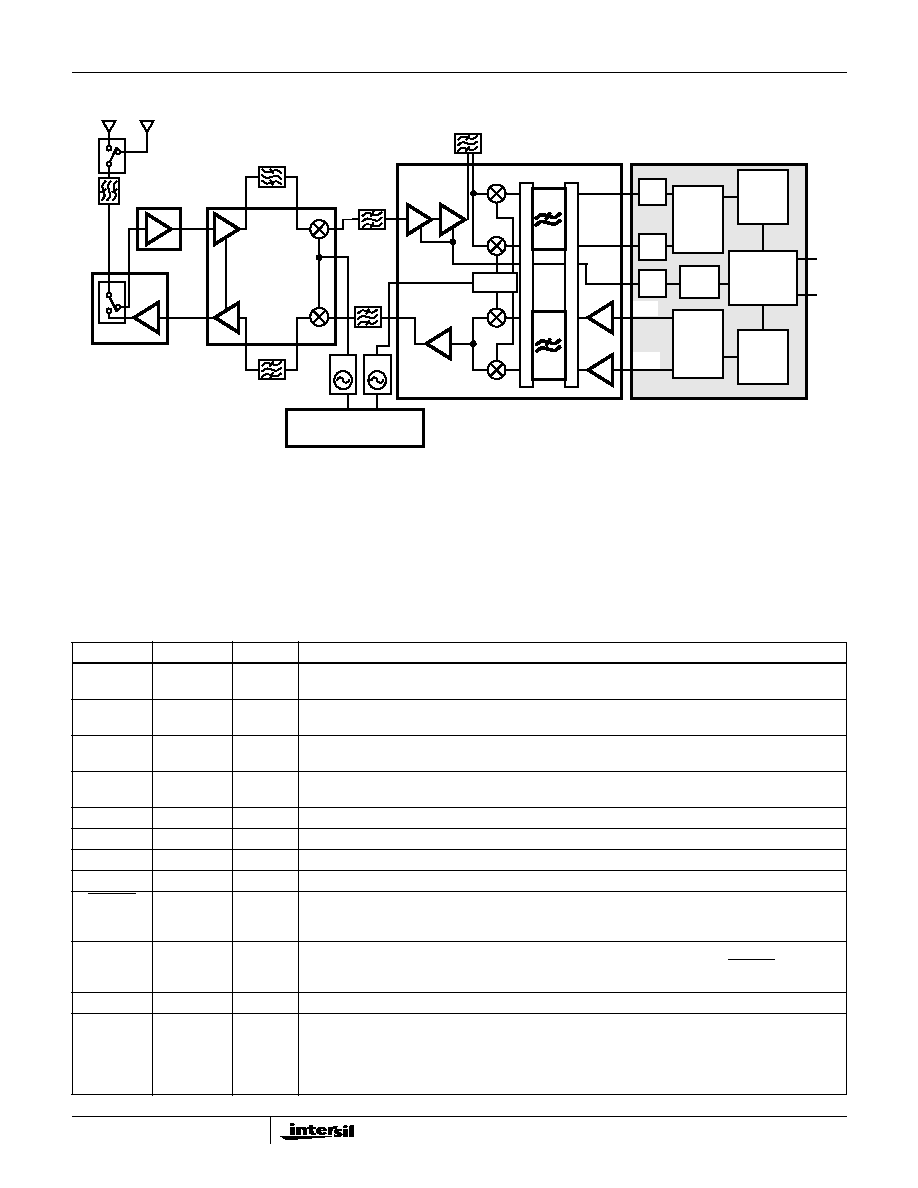
Typical Application Diagram
For additional information on the PRISMTM chip set, call
(407) 724-7800 to access Intersil' AnswerFAX system. When
prompted, key in the four-digit document number (File #) of
the data sheets you wish to receive.
The four-digit file numbers are shown in the Typical
Application Diagram, and correspond to the appropriate
circuit.
QUAD IF MODULATOR
RFPA
HFA3925
HFA3724/6
DSSS BASEBAND PROCESSOR
D
A
T
A
T
O
MA
C
CTRL
HFA3860A
HFA3524
0
o
/90
o
VCO
A/D
A/D
MAC-PHY
INTERFACE
802.11
VCO
DUAL SYNTHESIZER
HFA3624
UP/DOWN
CONVERTER
A/D
(FILE# 4067)
(FILE# 4488)
(FILE# 4062)
(FILE# 4066)
(FILE# 4132)
M
U
X
M
U
X
DEMOD
MOD.
DE-
SPREAD
SPREAD
Q
I
HFA3424
(NOTE)
(FILE# 4131)
TYPICAL TRANSCEIVER APPLICATION CIRCUIT USING THE HFA3860A
NOTE: Required for systems targeting 802.11 specifications.
CCA
RXI
RXQ
RSSI
TXI
TXQ
˜
2
Pin Descriptions
NAME
PIN
TYPE I/O
DESCRIPTION
V
DDA
(Analog)
10, 18, 20
Power
DC power supply 2.7V - 3.6V (Not Hardwired Together On Chip).
V
DD
(Digital)
7, 21, 29, 42
Power
DC power supply 2.7 - 3.6V
GND
(Analog)
11, 15, 19
Ground
DC power supply 2.7 - 3.6V, ground (Not Hardwired Together On Chip).
GND
(Digital)
6, 22, 31, 41
Ground
DC power supply 2.7 - 3.6V, ground.
V
REFN
17
I
"Negative" voltage reference for A/D's (I and Q) [Relative to V
REFP
]
V
REFP
16
I
"Positive" voltage reference for A/D's (I, Q and RSSI)
I
IN
12
I
Analog input to the internal 3-bit A/D of the In-phase received data.
Q
IN
13
I
Analog input to the internal 3-bit A/D of the Quadrature received data.
ANTSEL
26
O
The antenna select signal changes state as the receiver switches from antenna to antenna during the
acquisition process in the antenna diversity mode. This is a complement for ANTSEL (pin 27) for
differential drive of antenna switches.
ANTSEL
27
O
The antenna select signal changes state as the receiver switches from antenna to antenna during the
acquisition process in the antenna diversity mode. This is a complement for ANTSEL (pin 26) for
differential drive of antenna switches.
RSSI
14
I
Receive Signal Strength Indicator Analog input.
TX_PE
2
I
When active, the transmitter is configured to be operational, otherwise the transmitter is in standby mode.
TX_PE is an input from the external Media Access Controller (MAC) or network processor to the HFA3860A.
The rising edge of TX_PE will start the internal transmit state machine and the falling edge will initiate shut
down of the state machine. TX_PE envelopes the transmit data except for the last bit. The transmitter will
continue to run for 3 symbols after TX_PE goes inactive to allow the PA to shut down gracefully.
HFA3860A
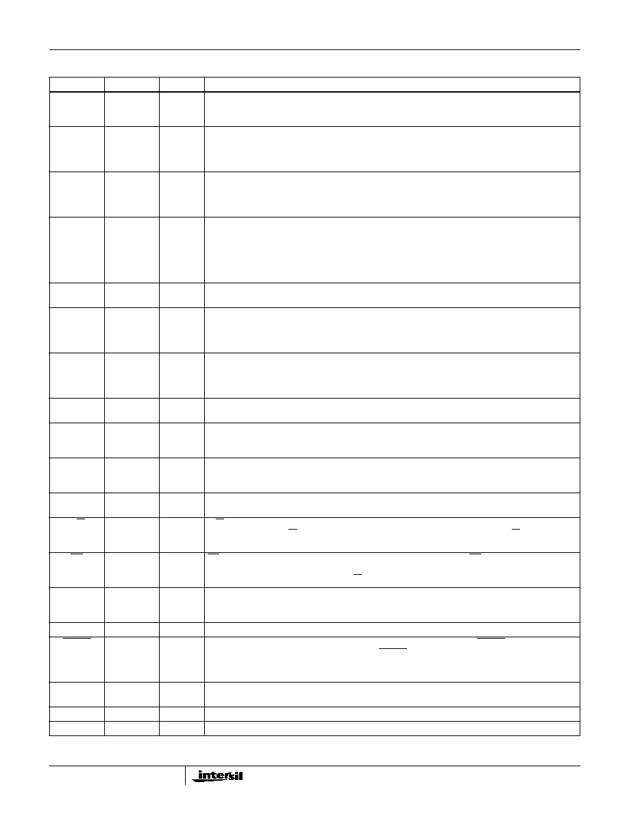
2-135
TXD
3
I
TXD is an input, used to transfer MAC Payload Data Unit (MPDU) data from the MAC or network
processor to the HFA3860A. The data is received serially with the LSB first. The data is clocked in the
HFA3860A at the rising edge of TXCLK.
TXCLK
4
O
TXCLK is a clock output used to receive the data on the TXD from the MAC or network processor to
the HFA3860A, synchronously. Transmit data on the TXD bus is clocked into the HFA3860A on the
rising edge. The clocking edge is also programmable to be on either phase of the clock. The rate of the
clock will be dependent upon the data rate that is programmed in the signalling field of the header.
TX_RDY
5
O
TX_RDY is an output to the external network processor indicating that Preamble and Header
information has been generated and that the HFA3860A is ready to receive the data packet from the
network processor over the TXD serial bus. The TX_RDY returns to the inactive state when the last chip
of the last symbol has been output.
CCA
32
O
Clear Channel Assessment (CCA) is an output used to signal that the channel is clear to transmit. The
CCA algorithm makes its decision as a function of RSSI, Energy detect (ED), and Carrier Sense (CRS).
The CCA algorithm and its features are described elsewhere in the data sheet.
Logic 0 = Channel is clear to transmit.
Logic 1 = Channel is NOT clear to transmit (busy).
This polarity is programmable and can be inverted.
RXD
35
O
RXD is an output to the external network processor transferring demodulated Header information and
data in a serial format. The data is sent serially with the LSB first. The data is frame aligned with MD_RDY.
RXCLK
36
O
RXCLK is the bit clock output. This clock is used to transfer Header information and payload data through
the RXD serial bus to the network processor. This clock reflects the bit rate in use. RXCLK is held to a
logic "0" state during the CRC16 reception. RXCLK becomes active after the SFD has been detected.
Data should be sampled on the rising edge. This polarity is programmable and can be inverted.
MD_RDY
34
O
MD_RDY is an output signal to the network processor, indicating header data and a data packet are
ready to be transferred to the processor. MD_RDY is an active high signal and it envelopes the data
transfer over the RXD serial bus. MD_RDY goes active when the SFD is detected and returns to its
inactive state when RX_PE goes inactive or an error is detected in the header.
RX_PE
33
I
When active, the receiver is configured to be operational, otherwise the receiver is in standby mode.
This is an active high input signal. In standby, RX_PE inactive, all A/D converters are disabled.
SD
25
I/O
SD is a serial bidirectional data bus which is used to transfer address and data to/from the internal registers.
The bit ordering of an 8-bit word is MSB first. The first 8 bits during transfers indicate the register address
immediately followed by 8 more bits representing the data that needs to be written or read at that register.
SCLK
24
I
SCLK is the clock for the SD serial bus. The data on SD is clocked at the rising edge. SCLK is an input
clock and it is asynchronous to the internal master clock (MCLK). The maximum rate of this clock is
11MHz or one half the master clock frequency, whichever is lower.
SDI
23
I
Serial Data Input in 3 wire mode described in Tech Brief 362. This pin is not used in the 4 wire interface
described in this data sheet. It should not be left floating.
R/W
8
I
R/W is an input to the HFA3860A used to change the direction of the SD bus when reading or writing
data on the SD bus. R/W also enables the serial shift register used in a read cycle. R/W must be set up
prior to the rising edge of SCLK. A high level indicates read while a low level is a write.
CS
9
I
CS is a Chip Select for the device to activate the serial control port. The CS doesn't impact any of the
other interface ports and signals, i.e., the TX or RX ports and interface signals. This is an active low
signal. When inactive SD, SCLK, and R/W become "don't care" signals.
TEST 7:0
37, 38, 39,
40, 43, 44,
45, 46
O
This is a data port that can be programmed to bring out internal signals or data for monitoring. These
bits are primarily reserved by the manufacturer for testing. A further description of the test port is given
at the appropriate section of this data sheet.
TEST_CK
1
O
This is the clock that is used in conjunction with the data that is being output from the test bus (TEST 0-7).
RESET
28
I
Master reset for device. When active TX and RX functions are disabled. If RESET is kept low the
HFA3860A goes into the power standby mode. RESET does not alter any of the configuration register
values nor does it preset any of the registers into default values. Device requires programming upon
power-up.
MCLK
30
I
Master Clock for device. The nominal frequency of this clock is 44MHz. This is used internally to gen-
erate all other internal necessary clocks and is divided by 2 or 4 for the transceiver clocks.
I
OUT
48
O
TX Spread baseband I digital output data. Data is output at the chip rate.
Q
OUT
47
O
TX Spread baseband Q digital output data. Data is output at the chip rate.
NOTE: Total of 48 pins; ALL pins are used.
Pin Descriptions
(Continued)
NAME
PIN
TYPE I/O
DESCRIPTION
HFA3860A