 | –≠–ª–µ–∫—Ç—Ä–æ–Ω–Ω—ã–π –∫–æ–º–ø–æ–Ω–µ–Ω—Ç: HFA3861 | –°–∫–∞—á–∞—Ç—å:  PDF PDF  ZIP ZIP |
1
File Number
4699.1
CAUTION: These devices are sensitive to electrostatic discharge; follow proper IC Handling Procedures.
http://www.intersil.com or 407-727-9207
|
Copyright
©
Intersil Corporation 1999
PRISM and PRISM logo are trademarks of Intersil Corporation.
A D V A N C E I N F O R M A T I O N
HFA3861
Direct Sequence Spread Spectrum
Baseband Processor
The Intersil HFA3861 Direct Sequence
Spread Spectrum (DSSS) baseband
processor is part of the PRISMÆ
2.4GHz radio chipset, and contains all
the functions necessary for a full or half duplex packet
baseband transceiver.
The HFA3861 has on-board A/D's for analog I and Q inputs
and outputs, for which the HFA3783 IF QMODEM is
recommended. Differential phase shift keying modulation
schemes DBPSK and DQPSK, with data scrambling
capability, are available along with Complementary Code
Keying to provide a variety of data rates. Built-in flexibility
allows the HFA3861 to be configured through a general
purpose control bus, for a range of applications. Both
Receive and Transmit AGC functions with 7-bit AGC control
obtain maximum performance in the analog portions of the
transceiver. The HFA3861 is housed in a thin plastic quad
flat package (TQFP) suitable for PCMCIA board
applications.
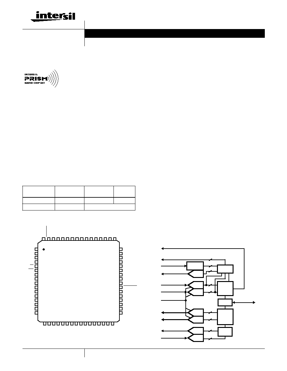
Pinout
Features
∑ Complete DSSS Baseband Processor
∑ Processing Gain . . . . . . . . . . . . . . . . . . . . FCC Compliant
∑ Programmable Data Rate. . . . . . . . 1, 2, 5.5, and 11Mbps
∑ Ultra Small Package . . . . . . . . . . . . . . . . . . . . . 10 x 10mm
∑ Single Supply Operation (44MHz Max) . . . . . 2.7V to 3.6V
∑ Modulation Methods . . . . . . . . DBPSK, DQPSK, and CCK
∑ Supports Full or Half Duplex Operations
∑ On-Chip A/D and D/A Converters for I/Q Data (6-Bit,
22MSPS), AGC, and Adaptive Power Control (7-Bit)
∑ Targeted for Multipath Delay Spreads ~100ns
∑ Supports Short Preamble Acquisition
Applications
∑ Enterprise WLAN Systems
∑ Systems Targeting IEEE 802.11 Standard
∑ DSSS PCMCIA Wireless Transceiver
∑ Spread Spectrum WLAN RF Modems
∑ TDMA Packet Protocol Radios
∑ Part 15 Compliant Radio Links
∑ Portable PDA/Notebook Computer
∑ Wireless Digital Audio, Video, Multimedia
∑ PCN/Wireless PBX
∑ Wireless Bridges
Simplified Block Diagram
Ordering Information
PART NO.
TEMP.
RANGE (
o
C)
PKG. TYPE
PKG. NO.
HFA3861IV
-40 to 85
64 Ld TQFP
Q64.10x10
HFA3861IV96
-40 to 85
Tape and Reel
TM
64 63 62 61 60 59 58 57 56 55 54 53 52 51 50 49
17 18 19 20 21 22 23 24 25 26 27 28 29 30 31 32
1
2
3
4
5
6
7
8
9
10
11
12
13
14
15
16
48
47
46
45
44
43
42
41
40
39
38
37
36
35
34
33
TEST4
TEST3
TEST2
TEST1
TEST0
GNDd
MCLK
NC
ANT-SEL
ANT-SEL
RX-RF_AGC
V
DDD
GNDd
TX_IF_AGC
RX_IF_AGC
COMPCAP1
GNDd
V
DDD
SD
SCLK
R/W
CS
GNDd
V
DDD
GNDa
RX_I+
RX_I-
V
DDA
RX_Q+
RX_Q-
GNDa
V
REF
SDI
RESET
TX_PE
RX_PE
CCA
TX_RD
Y
TXD
V
DDD
GNDd
TXCLK
MD_RD
Y
RXD
RXCLK
TEST7
TEST6
TEST5
V
DD
A
TX_A
GC_IN
RX-IF_DET
GNDa
I
REF
V
DD
A
TX_I+
TX_I-
GNDa
COMPCAP2
COMPRES2
GNDa
TX_Q+
TX_Q-
V
DD
A
COMPRES1
6
7
6
6
6
6
7
1
1
ANT_SEL
RX_RF_AGC
RX_IF_DET
THRESH.
DETECT
IF
DAC
I ADC
Q ADC
44MHz MCLK
HFA 3861 BBP
TX
ALC
TX
DAC
TX
ADC
I DAC
Q DAC
MOD
I/O
DEMOD
AGC
CTL
V
REF
RX_Q
±
RX_I
±
RX_IF_AGC
TX_Q
±
TX_I
±
TX_IF_AGC
TX_AGC_IN
DATA I/O
Data Sheet
July 1999

2
Table of Contents
PAGE
Pinout . . . . . . . . . . . . . . . . . . . . . . . . . . . . . . . . . . . . . . . . . . . . . . . . . . . . . . . . . . . . . . . . . . . . . . . . . . . . . . . . . . . . . . . . . . . .
1
Simplified Block Diagram . . . . . . . . . . . . . . . . . . . . . . . . . . . . . . . . . . . . . . . . . . . . . . . . . . . . . . . . . . . . . . . . . . . . . . . . . . . . .
1
Typical Application Diagram . . . . . . . . . . . . . . . . . . . . . . . . . . . . . . . . . . . . . . . . . . . . . . . . . . . . . . . . . . . . . . . . . . . . . . . . . . .
3
Pin Descriptions . . . . . . . . . . . . . . . . . . . . . . . . . . . . . . . . . . . . . . . . . . . . . . . . . . . . . . . . . . . . . . . . . . . . . . . . . . . . . . . . . . . .
4
External Interfaces . . . . . . . . . . . . . . . . . . . . . . . . . . . . . . . . . . . . . . . . . . . . . . . . . . . . . . . . . . . . . . . . . . . . . . . . . . . . . . . . . .
5
Control Port (4 Wire) . . . . . . . . . . . . . . . . . . . . . . . . . . . . . . . . . . . . . . . . . . . . . . . . . . . . . . . . . . . . . . . . . . . . . . . . . . . . . . . .
6
TX Port . . . . . . . . . . . . . . . . . . . . . . . . . . . . . . . . . . . . . . . . . . . . . . . . . . . . . . . . . . . . . . . . . . . . . . . . . . . . . . . . . . . . . . . . . . .
7
RX Port. . . . . . . . . . . . . . . . . . . . . . . . . . . . . . . . . . . . . . . . . . . . . . . . . . . . . . . . . . . . . . . . . . . . . . . . . . . . . . . . . . . . . . . . . . .
7
RX I/Q A/D Interface. . . . . . . . . . . . . . . . . . . . . . . . . . . . . . . . . . . . . . . . . . . . . . . . . . . . . . . . . . . . . . . . . . . . . . . . . . . . . . . . .
8
AGC Circuit . . . . . . . . . . . . . . . . . . . . . . . . . . . . . . . . . . . . . . . . . . . . . . . . . . . . . . . . . . . . . . . . . . . . . . . . . . . . . . . . . . . . . . .
8
RX_AGC_IN Interface . . . . . . . . . . . . . . . . . . . . . . . . . . . . . . . . . . . . . . . . . . . . . . . . . . . . . . . . . . . . . . . . . . . . . . . . . . . . . . .
8
TX I/Q DAC Interface . . . . . . . . . . . . . . . . . . . . . . . . . . . . . . . . . . . . . . . . . . . . . . . . . . . . . . . . . . . . . . . . . . . . . . . . . . . . . . . .
9
Test Port . . . . . . . . . . . . . . . . . . . . . . . . . . . . . . . . . . . . . . . . . . . . . . . . . . . . . . . . . . . . . . . . . . . . . . . . . . . . . . . . . . . . . . . . . .
9
Power Down Modes . . . . . . . . . . . . . . . . . . . . . . . . . . . . . . . . . . . . . . . . . . . . . . . . . . . . . . . . . . . . . . . . . . . . . . . . . . . . . . . . .
9
Transmitter Description. . . . . . . . . . . . . . . . . . . . . . . . . . . . . . . . . . . . . . . . . . . . . . . . . . . . . . . . . . . . . . . . . . . . . . . . . . . . . . .
9
Header/Packet Description. . . . . . . . . . . . . . . . . . . . . . . . . . . . . . . . . . . . . . . . . . . . . . . . . . . . . . . . . . . . . . . . . . . . . . . . . . . .
10
Scrambler and Data Encoder Description . . . . . . . . . . . . . . . . . . . . . . . . . . . . . . . . . . . . . . . . . . . . . . . . . . . . . . . . . . . . . . . .
12
Spread Spectrum Modulator Description . . . . . . . . . . . . . . . . . . . . . . . . . . . . . . . . . . . . . . . . . . . . . . . . . . . . . . . . . . . . . . . . . . . .
12
CCK Modulation . . . . . . . . . . . . . . . . . . . . . . . . . . . . . . . . . . . . . . . . . . . . . . . . . . . . . . . . . . . . . . . . . . . . . . . . . . . . . . . . . . . .
12
TX Power Control . . . . . . . . . . . . . . . . . . . . . . . . . . . . . . . . . . . . . . . . . . . . . . . . . . . . . . . . . . . . . . . . . . . . . . . . . . . . . . . . . . .
13
Clear Channel Assessment (CCA) and Energy Detect (ED) Description. . . . . . . . . . . . . . . . . . . . . . . . . . . . . . . . . . . . . . . . .
13
AGC Description. . . . . . . . . . . . . . . . . . . . . . . . . . . . . . . . . . . . . . . . . . . . . . . . . . . . . . . . . . . . . . . . . . . . . . . . . . . . . . . . . . . .
14
Demodulator Description . . . . . . . . . . . . . . . . . . . . . . . . . . . . . . . . . . . . . . . . . . . . . . . . . . . . . . . . . . . . . . . . . . . . . . . . . . . . .
14
Acquisition Description . . . . . . . . . . . . . . . . . . . . . . . . . . . . . . . . . . . . . . . . . . . . . . . . . . . . . . . . . . . . . . . . . . . . . . . . . . . . . . .
15
PN Correlators Description . . . . . . . . . . . . . . . . . . . . . . . . . . . . . . . . . . . . . . . . . . . . . . . . . . . . . . . . . . . . . . . . . . . . . . . . . . .
16
Data Demodulation and Tracking Description (DBPSK and DQPSK Modes) . . . . . . . . . . . . . . . . . . . . . . . . . . . . . . . . . . . . .
17
Data Decoder and Descrambler Description . . . . . . . . . . . . . . . . . . . . . . . . . . . . . . . . . . . . . . . . . . . . . . . . . . . . . . . . . . . . . . . . . . . .
17
Data Demodulation in the CCK Modes . . . . . . . . . . . . . . . . . . . . . . . . . . . . . . . . . . . . . . . . . . . . . . . . . . . . . . . . . . . . . . . . . .
19
Tracking . . . . . . . . . . . . . . . . . . . . . . . . . . . . . . . . . . . . . . . . . . . . . . . . . . . . . . . . . . . . . . . . . . . . . . . . . . . . . . . . . . . . . . . . . .
19
Demodulator Performance . . . . . . . . . . . . . . . . . . . . . . . . . . . . . . . . . . . . . . . . . . . . . . . . . . . . . . . . . . . . . . . . . . . . . . . . . . . .
19
Overall Eb/N0 Versus BER Performance . . . . . . . . . . . . . . . . . . . . . . . . . . . . . . . . . . . . . . . . . . . . . . . . . . . . . . . . . . . . . . . . .
19
Clock Offset Tracking Performance . . . . . . . . . . . . . . . . . . . . . . . . . . . . . . . . . . . . . . . . . . . . . . . . . . . . . . . . . . . . . . . . . . . . .
20
Carrier Offset Frequency Performance . . . . . . . . . . . . . . . . . . . . . . . . . . . . . . . . . . . . . . . . . . . . . . . . . . . . . . . . . . . . . . . . . .
20
A Default Register Configuration . . . . . . . . . . . . . . . . . . . . . . . . . . . . . . . . . . . . . . . . . . . . . . . . . . . . . . . . . . . . . . . . . . . . . . .
21
Control Registers . . . . . . . . . . . . . . . . . . . . . . . . . . . . . . . . . . . . . . . . . . . . . . . . . . . . . . . . . . . . . . . . . . . . . . . . . . . . . . . . . . .
23
Test Circuit . . . . . . . . . . . . . . . . . . . . . . . . . . . . . . . . . . . . . . . . . . . . . . . . . . . . . . . . . . . . . . . . . . . . . . . . . . . . . . . . . . . . . . . .
33
Waveforms . . . . . . . . . . . . . . . . . . . . . . . . . . . . . . . . . . . . . . . . . . . . . . . . . . . . . . . . . . . . . . . . . . . . . . . . . . . . . . . . . . . . . . . .
33
Thin Plastic Quad Flatpack Packages (TQFP) . . . . . . . . . . . . . . . . . . . . . . . . . . . . . . . . . . . . . . . . . . . . . . . . . . . . . . . . . . . . .
35
HFA3861
3
HF
A3861
Typical Application Diagram
For additional information on the PRISMÆ chip set, call (407) 724-7800 to access
Intersil' AnswerFAX system. When prompted, key in the four-digit document
number (File #) of the data sheets you wish to receive.
The four-digit file numbers are shown in the Typical Application Diagram, and
correspond to the appropriate circuit.
TYPICAL TRANSCEIVER APPLICATION CIRCUIT USING THE HFA3861
6
7
6
6
6
6
7
1
1
IF
DAC
I ADC
Q ADC
44MHz MCLK
HFA3861 BBP
TX
ALC
TX
DAC
TX
ADC
I DAC
Q DAC
MOD
I/O
DEMOD
AGC
CTL
IF
RF
ADC
RF
DAC
REF IN
LO
I/O LO
PLL
HFA3783 QUAD IF
REF IN
REF IN
RF
LO
PLL
HFA3683 RF/IF
CONV
HFA3963
RFPA
DIFFERENTIAL SIGNALS
REFOUT
EXTERNAL
MEMORY
RADIO
DATA
INTERFACE
RADIO
CONTROL
PORTS
GP SERIAL
PORTS
WEP
ENGINE
CPU
16-BIT
PIPELINED
CONTROL
PROCESSOR
HOST
INTERFACE
LOGIC
MEMORY
ACCESS
ARBITER
HOSTPC
INTERF
A
C
E
HFA3841
MAC
4
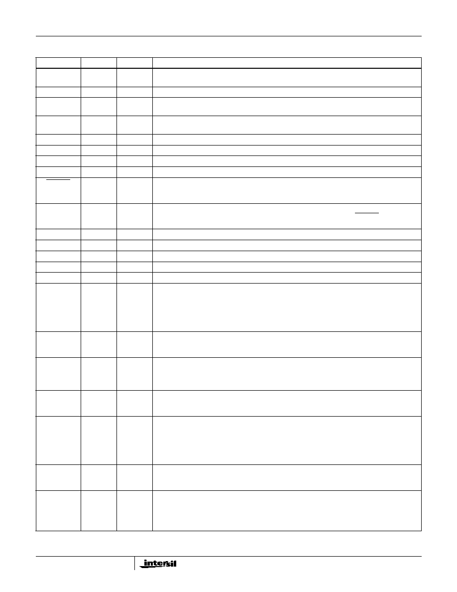
Pin Descriptions
NAME
PIN
TYPE I/O
DESCRIPTION
V
DDA
(Analog)
12, 17, 22,
31
Power
DC power supply 2.7V - 3.6V (Not Hard wired Together On Chip).
V
DDD
(Digital)
2, 8, 37, 57
Power
DC power supply 2.7 - 3.6V
GNDa
(Analog)
9, 15, 20,
25, 28,
Ground
DC power supply 2.7 - 3.6V, ground (Not Hard wired Together On Chip).
GNDd (Digital) 1, 7, 36, 43,
56
Ground
DC power supply 2.7 - 3.6V, ground.
V
REF
16
I
Voltage reference for A/D's and D/A's
I
REF
21
I
Current reference for internal ADC and DAC devices. Requires a 12k
resistor to ground.
RXI
, +/-
10/11
I
Analog input to the internal 6-bit A/D of the In-phase received data. Balanced differential 10+/11-
RXQ
, +/-
13/14
I
Analog input to the internal 6-bit A/D of the Quadrature received data. Balanced differential 13+/14-
ANTSEL
39
O
The antenna select signal changes state as the receiver switches from antenna to antenna during the
acquisition process in the antenna diversity mode. This is a complement for ANTSEL (pin 40) for
differential drive of antenna switches.
ANTSEL
40
O
The antenna select signal changes state as the receiver switches from antenna to antenna during the
acquisition process in the antenna diversity mode. This is a complement for ANTSEL (pin 39) for
differential drive of antenna switches.
RX_IF_DET
19
I
Analog input to the receive power A/D converter for AGC control.
RX_IF_AGC
34
O
Analog drive to the IF AGC control.
RX_RF_AGC
38
O
Drive to the RF AGC stage attenuator. CMOS digital.
TX_AGC_IN
18
I
Input to the transmit power A/D converter for transmit AGC control.
TX_IF_AGC
35
O
Analog drive to the transmit IF power control.
TX_PE
62
I
When active, the transmitter is configured to be operational, otherwise the transmitter is in standby
mode. TX_PE is an input from the external Media Access Controller (MAC) or network processor to
the HFA3861. The rising edge of TX_PE will start the internal transmit state machine and the falling
edge will initiate shut down of the state machine. TX_PE envelopes the transmit data except for the
last bit. The transmitter will continue to run for 4
µ
s after TX_PE goes inactive to allow the PA to shut
down gracefully.
TXD
58
I
TXD is an input, used to transfer MAC Payload Data Unit (MPDU) data from the MAC or network
processor to the HFA3861. The data is received serially with the LSB first. The data is clocked in the
HFA3861 at the rising edge of TXCLK.
TXCLK
55
O
TXCLK is a clock output used to receive the data on the TXD from the MAC or network processor to
the HFA3861, synchronously. Transmit data on the TXD bus is clocked into the HFA3861 on the rising
edge. The clocking edge is also programmable to be on either phase of the clock. The rate of the clock
will be dependent upon the data rate that is programmed in the signalling field of the header.
TX_RDY
59
O
TX_RDY is an output to the external network processor indicating that Preamble and Header
information has been generated and that the HFA3861 is ready to receive the data packet from the
network processor over the TXD serial bus.
CCA
60
O
Clear Channel Assessment (CCA) is an output used to signal that the channel is clear to transmit. The
CCA may be configured to one of four possible algorithms. The CCA algorithm and its features are
described elsewhere in the data sheet.
Logic 0 = Channel is clear to transmit.
Logic 1 = Channel is NOT clear to transmit (busy).
This polarity is programmable and can be inverted.
RXD
53
O
RXD is an output to the external network processor transferring demodulated Header information and
data in a serial format. The data is sent serially with the LSB first. The data is frame aligned with
MD_RDY.
RXCLK
52
O
RXCLK is the bit clock output. This clock is used to transfer Header information and payload data
through the RXD serial bus to the network processor. This clock reflects the bit rate in use. RXCLK is
held to a logic "0" state during the CRC16 reception. RXCLK becomes active after the SFD has been
detected. Data should be sampled on the rising edge. This polarity is programmable and can be
inverted.
HFA3861
5
External Interfaces
There are three primary digital interface ports for the
HFA3861 that are used for configuration and during normal
operation of the device as shown in Figure 1. These ports
are:
∑ The Control Port, which is used to configure, write
and/or read the status of the internal HFA3861
registers.
∑ The TX Port, which is used to accept the data that
needs to be transmitted from the network processor.
∑ The RX Port, which is used to output the received
demodulated data to the network processor.
In addition to these primary digital interfaces the device
includes a byte wide parallel Test Port which can be
configured to output various internal signals and/or data.
The device can also be set into various power consumption
modes by external control. The HFA3861 contains four
Analog to Digital (A/D) converters and four Digital to Analog
converters. The analog interfaces to the HFA3861 include,
the In phase (I) and quadrature (Q) data component inputs/
outputs, and the RF and IF receive automatic gain control
and transmit output power control.
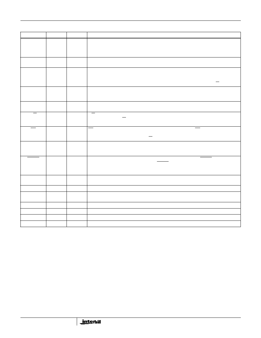
MD_RDY
54
O
MD_RDY is an output signal to the network processor, indicating header data and a data packet are
ready to be transferred to the processor. MD_RDY is an active high signal that signals the start of data
transfer over the RXD serial bus. MD_RDY goes active when the SFD (Note) is detected and returns
to its inactive state when RX_PE goes inactive or an error is detected in the header.
RX_PE
61
I
When active, the receiver is configured to be operational, otherwise the receiver is in standby mode.
This is an active high input signal. In standby, RX_PE inactive, all RX A/D converters are disabled.
SD
3
I/O
SD is a serial bidirectional data bus which is used to transfer address and data to/from the internal
registers. The bit ordering of an 8-bit word is MSB first. The first 8 bits during transfers indicate the
register address immediately followed by 8 more bits representing the data that needs to be written
or read at that register. In the 4 wire interface mode, this pin is tristated unless the R/W pin is high.
SCLK
4
I
SCLK is the clock for the SD serial bus. The data on SD is clocked at the rising edge. SCLK is an input
clock and it is asynchronous to the internal master clock (MCLK). The maximum rate of this clock is
11MHz or one half the master clock frequency, whichever is lower.
SDI
64
I
Serial Data Input in 3 wire mode described in Tech Brief TBD. This pin is not used in the 4 wire
interface described in this data sheet. It should not be left floating.
R/W
5
I
R/W is an input to the HFA3861 used to change the direction of the SD bus when reading or writing
data on the SD bus. R/W must be set up prior to the rising edge of SCLK. A high level indicates read
while a low level is a write.
CS
6
I
CS is a Chip select for the device to activate the serial control port. The CS doesn't impact any of the
other interface ports and signals, i.e., the TX or RX ports and interface signals. This is an active low
signal. When inactive SD, SCLK, and R/W become "don't care" signals.
TEST 7:0
51, 50, 49,
48, 47, 46,
45, 44
I/O
This is a data port that can be programmed to bring out internal signals or data for monitoring. These
bits are primarily reserved by the manufacturer for testing. A further description of the test port is given
in the appropriate section of this data sheet.
RESET
63
I
Master reset for device. When active TX and RX functions are disabled. If RESET is kept low the
HFA3861 goes into the power standby mode. RESET does not alter any of the configuration register
values nor does it preset any of the registers into default values. Device requires programming upon
power-up.
MCLK
42
I
Master Clock for device. The nominal frequency of this clock is 44MHz. This is used internally to
generate all other internal necessary clocks and is divided by 2 or 4 for the transceiver clocks.
TXI
+/-
23/24
O
TX Spread baseband I digital output data. Data is output at the chip rate. Balanced differential 23+/ 24-
TXQ
+/-
29/30
O
TX Spread baseband Q digital output data. Data is output at the chip rate. Balanced differential
29+/30-.
CompCap
33
I
Compensation capacitor
CompCap2
26
I
Compensation capacitor
CompRes1
32
I
Compensation Resistor
CompRes2
27
I
Compensation Resistor
NOTE: See CR10<3>.
Pin Descriptions
(Continued)
NAME
PIN
TYPE I/O
DESCRIPTION
HFA3861