 | –≠–ª–µ–∫—Ç—Ä–æ–Ω–Ω—ã–π –∫–æ–º–ø–æ–Ω–µ–Ω—Ç: HFA3925 | –°–∫–∞—á–∞—Ç—å:  PDF PDF  ZIP ZIP |

2-179
HFA3925
2.4GHz - 2.5GHz 250mW Power Amplifier
The Intersil 2.4GHz PRISMTM chip set
is a highly integrated five-chip solution
for RF modems employing Direct
Sequence Spread Spectrum (DSSS)
signaling. The HFA3925 2.4GHz-
2.5GHz, 250mW power amplifier is one of the five chips in
the PRISMTM chip set (see the Typical Application Diagram).
The Intersil HFA3925 is an integrated power amplifier with
transmit/receive switch in a low cost SSOP 28 plastic
package. The power amplifier delivers +27dB of gain with
high efficiency and can be operated with voltages as low as
2.7V. The power amplifier switch is fully monolithic and can
be controlled with CMOS logic levels.
The HFA3925 is ideally suited for QPSK, BPSK or other
linearly modulated systems in the 2.4GHz Industrial,
Scientific, and Medical (ISM) frequency band. It can also be
used in GFSK systems where levels of +25dBm are
required. Typical applications include Wireless Local Area
Network (WLAN) and wireless portable data collection.
REMEMBER: Always apply Negative power to the VG
pins before applying the Positive V
DD
bias. Failure to do
so may result in the destruction of the HFA3925 Power
Amplifier.
Features
∑ Highly Integrated Power Amplifier with T/R Switch
∑ Operates Over 2.7V to 6V Supply Voltage
∑ High Linear Output Power (P
1dB
: +24dBm)
∑ Individual Gate Control for Each Amplifier Stage
∑ Low Cost SSOP-28 Plastic Package
Applications
∑ Systems Targeting IEEE 802.11 Standard
∑ TDD Quadrature-Modulated Communication Systems
∑ Wireless Local Area Networks
∑ PCMCIA Wireless Transceivers
∑ ISM Systems
∑ TDMA Packet Protocol Radios
∑ PCS/Wireless PBX
TM
Ordering Information
PART NUMBER
TEMP.
RANGE (
o
C)
PACKAGE
PKG.
NO.
HFA3925IA
-40 to 85
28 Ld SSOP
M28.15
HFA3925IA96
-40 to 85
Tape and Reel
Pinout
HFA3925
(SSOP)
TOP VIEW
Functional Block Diagram
GND
RF OUT
V
DD3
GND
GND
GND
GND
V
DD
TR
V
G3
GND
GND
GND
GND
GND
RX OUT
GND
V
G2
GND
GND
GND
V
DD1
GND
V
G1
T/R CNTRL
GND
V
DD2
GND
RF IN
28
27
26
25
24
23
22
21
20
19
18
17
16
15
1
2
3
4
5
6
7
8
9
10
11
12
13
14
STAGE BIAS CONTROL
V
DDX
(+)
RF IN
STAGE 1
STAGE 2
STAGE 3
T/R CNTRL
RF_OUT
RX OUT
V
GX
(-)
TO
ANTENNA
Data Sheet
July 1998
File Number
4132.4
CAUTION: These devices are sensitive to electrostatic discharge; follow proper IC Handling Procedures.
http://www.intersil.com or 407-727-9207
|
Copyright
©
Intersil Corporation 1999
PRISMÆ is a registered trademark of Intersil Corporation. PRISM logo is a trademark of Intersil Corporation.
2-180
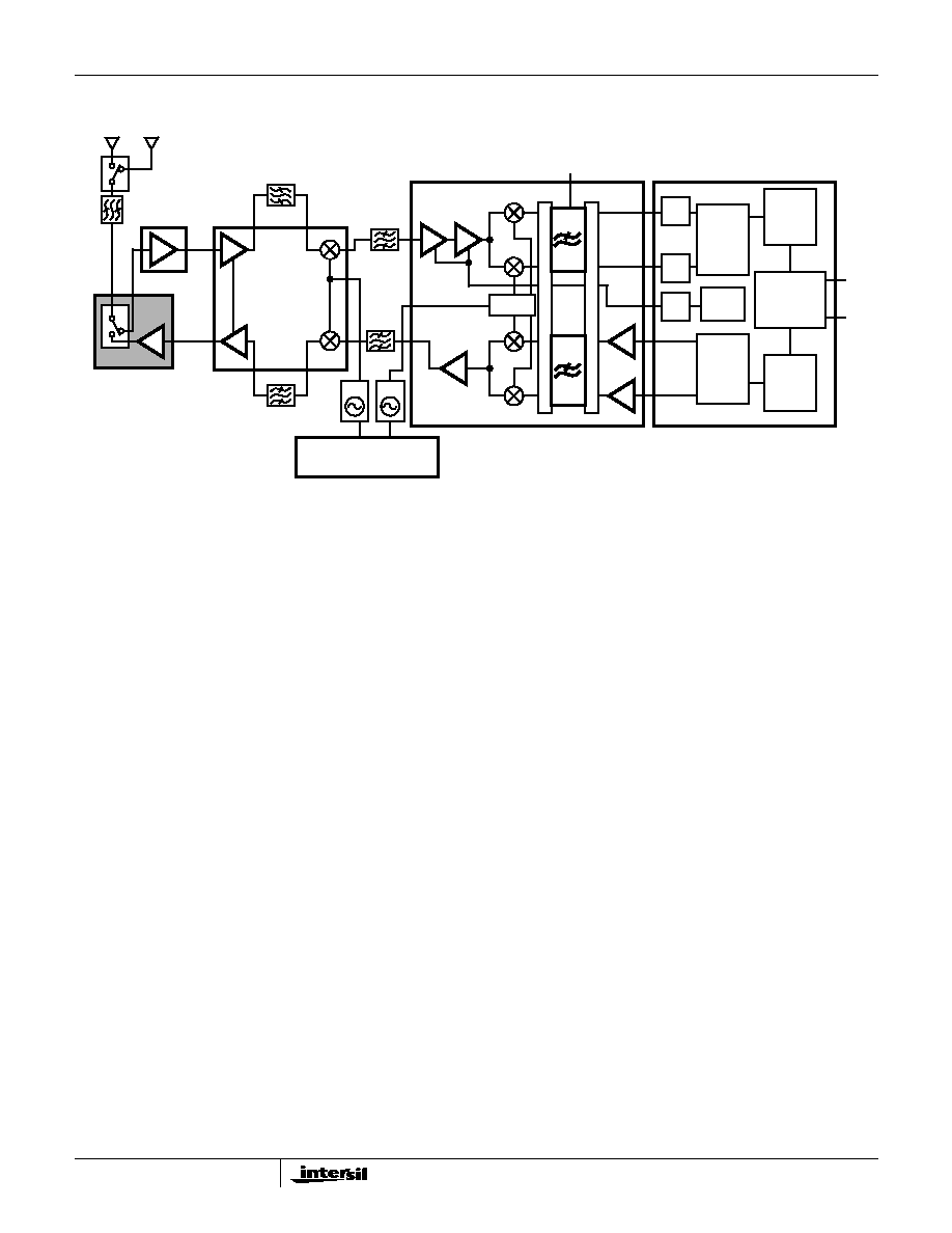
Typical Application Diagram
For additional information on the PRISMTM chip set, call
(407) 724-7800 to access Intersil AnswerFAX system. When
prompted, key in the four-digit document number (File #) of
the datasheets you wish to receive.
The four-digit file numbers are shown in the Typical
Application Diagram, and correspond to the appropriate
circuit
QUAD IF MODULATOR
RFPA
HFA3925
HFA3724
DSSS BASEBAND PROCESSOR
D
A
T
A
T
O
MA
C
CTRL
HSP3824
TUNE/SELECT
HFA3524
0
o
/90
o
VCO
A/D
A/D
MAC-PHY
INTERFACE
802.11
VCO
DUAL SYNTHESIZER
HFA3624
UP/DOWN
CONVERTER
A/D
(FILE# 4067)
(FILE# 4064)
(FILE# 4062)
(FILE# 4066)
(FILE# 4132)
PRISMTM CHIP SET FILE #4063
M
U
X
M
U
X
DPSK
DEMOD
DPSK
MOD.
DE-
SPREAD
SPREAD
Q
I
HFA3424
(NOTE)
(FILE# 4131)
CCA
RXI
RXQ
RSSI
TXI
TXQ
˜
2
TYPICAL TRANSCEIVER APPLICATION USING THE HFA3925
NOTE: Required for systems targeting 802.11 specifications.
HFA3925

2-181
Absolute Maximum Ratings
Thermal Information
Maximum Input Power (Note 2) . . . . . . . . . . . . . . . . . . . . . . +23dBm
Operating Voltages (Notes 2, 3). . . . . . . . . . . . V
DD
= 8V, V
GG
= -8V
Operating Conditions
Temperature Range . . . . . . . . . . . . . . . . . . . . . . . . . . -40
o
C to 85
o
C
Thermal Resistance (Typical, Note 1)
JA
(
o
C/W)
SSOP Package . . . . . . . . . . . . . . . . . . . . . . . . . . . .
88
Maximum Storage Temperature Range . . . . . . . . . . -65
o
C to 150
o
C
CAUTION: Stresses above those listed in "Absolute Maximum Ratings" may cause permanent damage to the device. This is a stress only rating and operation of the
device at these or any other conditions above those indicated in the operational sections of this specification is not implied.
NOTE:
1.
JA
is measured with the component mounted on an evaluation PC board in free air.
Electrical Specifications
T
A
= 25
o
C, Z
0
= 50
, V
DD
= +5V, P
IN
= -30dBm, f = 2.45GHz, Unless Otherwise Specified
PARAMETER
MIN
TYP
MAX
UNITS
POWER AMPLIFIER
Linear Gain
27
28
32
dB
VSWR In/Out
-
1.75:1
-
Input Return Loss
-
-11.3
-
dB
Output Return Loss
-
-11.3
-
dB
Output Power at P
1dB
22.5
24.5
-
dBm
Second Harmonic at P
1dB
-
-20
0
dBc
Third Harmonic at P
1dB
-
-30
-10
dBc
IDD at P1dB (VDD1 + VDD2 + VDD3)
-
270
375
mA
NOTES:
2. Ambient temperature (T
A
) = 25
o
C.
3. |V
DD
| + |V
GG
| not to exceed 12V.
Pin Description
PINS
SYMBOL
DESCRIPTION
1
GND
DC and RF Ground.
2
GND
DC and RF Ground.
3
GND
DC and RF Ground.
4
GND
DC and RF Ground.
5
GND
DC and RF Ground.
6
GND
DC and RF Ground.
7
GND
DC and RF Ground.
8
RX OUT
Output of T/R Switch for receive mode.
9
V
G2
Negative bias control for the second PA stage, adjusted to set V
DD2
quiescent bias current, which is typi-
cally 53mA. Typical voltage at pin = -0.75V. Input impedance: > 1M
.
10
GND
DC and RF Ground.
11
V
DD1
Positive bias for the first stage of the PA, 2.7V to 6V.
12
GND
DC and RF Ground.
13
GND
DC and RF Ground.
14
V
G1
Negative bias control for the first PA stage, adjusted to set V
DD1
quiescent bias current, which is typically
20mA. Typical voltage at pin = -0.75V. Input impedance: > 1M
.
15
RF IN
RF Input of the Power Amplifier.
16
GND
DC and RF Ground.
HFA3925
2-182
17
V
G3
Negative bias control for the third PA stage, adjusted to set V
DD3
quiescent bias current, which is typically
90mA. Typical voltage at pin = -0.95V. Input impedance: > 1M
.
18
V
DD2
Positive bias for the second stage of the PA. 2.7V to 6V.
19-22
GND
DC and RF Ground.
23
V
DD3
Positive bias for the third stage of the PA. 2.7V to 6V.
24
GND
DC and RF Ground.
25
RF OUT
RF output of T/R switch and power amplifier for transmit mode.
26
T/R CTRL
0V for transmit mode, +5V for receive mode. Low < = 0.2V, high > = V
DD
-0.2V.
27
V
DD
TR
V
DD
for T/R switch.
28
GND
DC and RF Ground.
NOTE: Process variation will effect V
G3
voltage requirement to develop 90mA stage 3 quiescent current, maximum range = -0.69V to -1.04V.
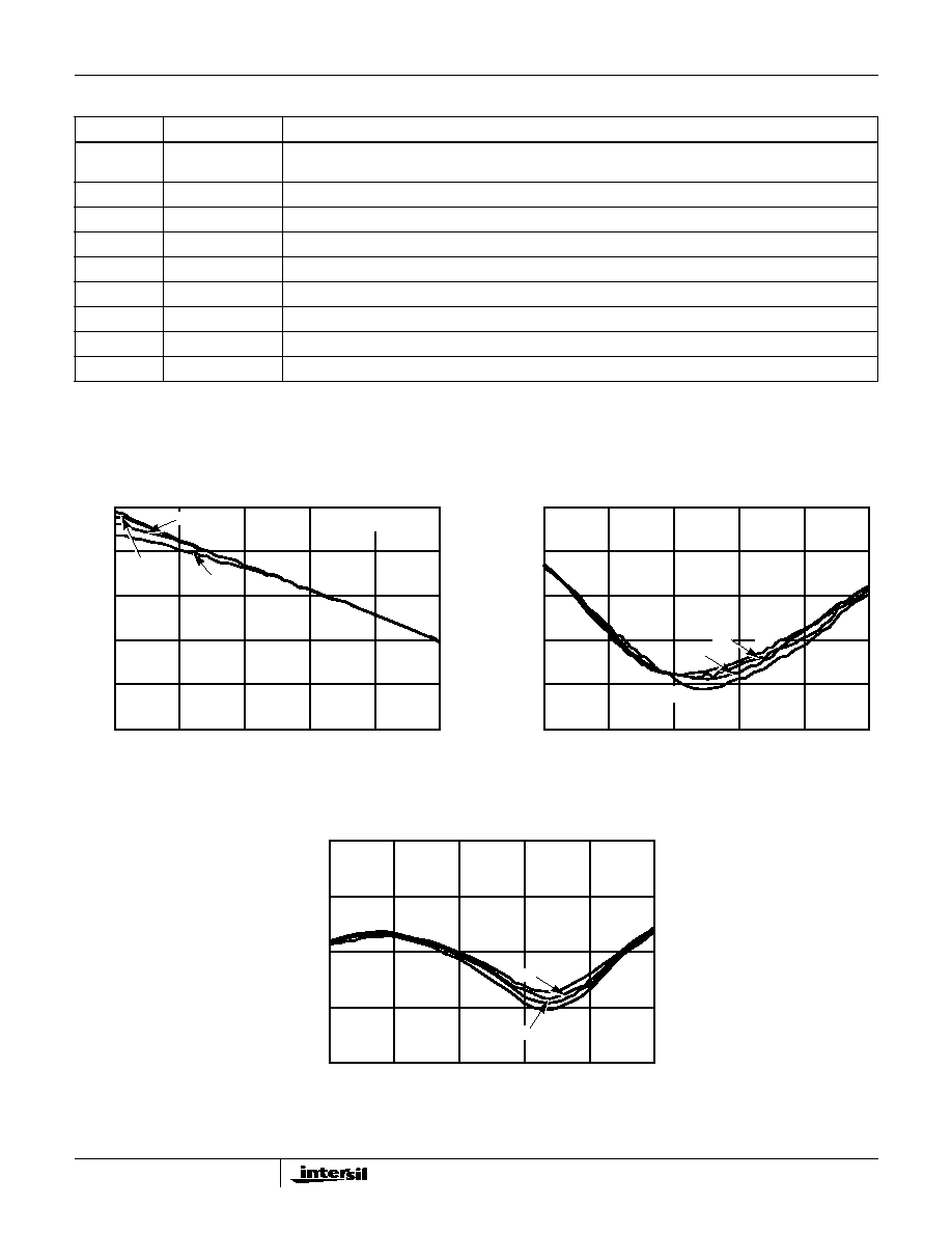
Typical Performance Curves
Power Amplifier Small Signal Performance
NOTE: All data measured at T
A
= 25
o
C and V
G1
, V
G2
and V
G3
adjusted for first stage quies-
cent current of 20mA, second stage current of 53mA and third stage current of 90mA, respectively
FIGURE 1. LINEAR GAIN
FIGURE 2. INPUT MATCH
FIGURE 3. OUTPUT MATCH
Pin Description
(Continued)
PINS
SYMBOL
DESCRIPTION
6V
2.0
2.2
2.4
2.6
2.8
3.0
35
25
20
15
10
FREQUENCY (GHz)
GAIN (dB)
30
V
DD1
= V
DD2
= V
DD3
5V
3V
4V
6V
2.0
2.2
2.4
2.6
2.8
3.0
-5
-15
-20
-25
-30
FREQUENCY (GHz)
RETURN LOSS (dB)
-10
5V
3V
4V
6V
2.0
2.2
2.4
2.6
2.8
3.0
0
-5
-10
-15
-20
FREQUENCY (GHz)
RETURN LOSS (dB)
5V
3V
4V
HFA3925
2-183
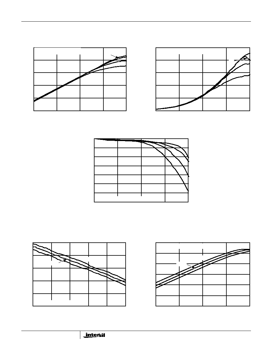
Power Amplifier CW Performance at Various Supply Voltages
NOTE: All data measured at T
A
= 25
o
C and V
G1
, V
G2
and V
G3
adjusted for first stage quiescent current of 20mA, second stage current of 53mA and third stage current of 90mA, respectively.
FIGURE 4. POWER OUTPUT
FIGURE 5. POWER ADDED EFFICIENCY
FIGURE 6. GAIN COMPRESSION
Power Amplifier Temperature Performance
NOTE: All data measured at T
A
= 25
o
C and V
G1
, V
G2
and V
G3
adjusted for first stage quies-
cent current of 20mA, second stage current of 53mA and third stage current of 90mA, respectively.
FIGURE 7. LINEAR GAIN
FIGURE 8. POWER OUTPUT
Typical Performance Curves
(Continued)
6V
-19
-14
-9
-4
1
30
20
15
10
5
POWER INPUT (dBm)
PO
WER (dBm)
25
2.45GHz, V
DD1
= V
DD2
= V
DD3
5V
3V
4V
6V
-19
-14
-9
-4
1
50
30
20
10
0
INPUT POWER (dBm)
EFFICIENCY (%)
40
5V
3V
4V
2.45GHz, V
DD1
= V
DD2
= V
DD3
6V
0
-2
-3
-4
-7
INPUT POWER (dBm)
COMPRESSION (dBm)
-1
5V
3V
4V
2.45GHz, V
DD1
= V
DD2
= V
DD3
-5
-6
-19
-14
-9
-4
1
2.0
2.2
2.4
2.6
2.8
3.0
35
25
20
15
10
FREQUENCY (GHz)
GAIN (dB)
30
25
o
C
70
o
C
V
DD1
= V
DD2
= V
DD3
= +5V
-20
o
C
-19
-14
-9
-4
1
30
20
15
10
0
INPUT POWER (dBm)
PO
WER (dBm)
25
2.45GHz, V
DD1
= V
DD2
= V
DD3
= +5V
5
70
o
C
-20
o
C
25
o
C
HFA3925