 | –≠–ª–µ–∫—Ç—Ä–æ–Ω–Ω—ã–π –∫–æ–º–ø–æ–Ω–µ–Ω—Ç: HFA3926IA | –°–∫–∞—á–∞—Ç—å:  PDF PDF  ZIP ZIP |

2-229
HFA3926
2.0GHz - 2.7GHz 250mW Power Amplifier
The Intersil HFA3926 is an integrated
power amplifier in a low cost SSOP 28
plastic package. The power amplifier
delivers +27dB of gain with high
efficiency and can be operated with
voltages as low as 2.7V.
The HFA3926 is ideally suited for QPSK, BPSK or other
linearly modulated systems in the 2.4GHz Industrial,
Scientific, and Medical (ISM) frequency band. It can also be
used in GFSK systems where levels of +25dBm are
required. Typical applications include Wireless Local Area
Network (WLAN) and Wireless Local Loop systems.
REMEMBER: Always apply Negative power to the VG pins
before applying the Positive V
DD
bias. Failure to do so may
result in the destruction of the HFA3926 Power Amplifier.
Pinout
HFA3926
(SSOP)
TOP VIEW
Features
∑ Highly Integrated Power Amplifier
∑ Operates Over 2.7V to 6V Supply Voltage
∑ High Linear Output Power (P
1dB
: +24.5dBm)
∑ Low Cost SSOP-28 Plastic Package
Applications
∑ Wireless Local Loop Systems
∑ Systems Targeting IEEE 802.11 Standard
∑ TDD Quadrature-Modulated Communication Systems
∑ Wireless Local Area Networks
∑ PCMCIA Wireless Transceivers
∑ ISM Systems
Functional Block Diagram
Ordering Information
PART NUMBER
TEMP.
RANGE (
o
C)
PACKAGE
PKG.
NO.
HFA3926IA
-40 to 85
28 Ld SSOP
M28.15
HFA3926IA96
-40 to 85
Tape and Reel
TM
GND
RF OUT
V
DD3
GND
GND
GND
GND
V
DD
V
G3
GND
GND
GND
GND
GND
N/C
GND
V
G2
GND
GND
GND
V
DD1
GND
V
G1
GND
GND
V
DD2
GND
RF IN
28
27
26
25
24
23
22
21
20
19
18
17
16
15
1
2
3
4
5
6
7
8
9
10
11
12
13
14
STAGE BIAS CONTROL
V
DDX
(+)
RF IN
STAGE 1
STAGE 2
STAGE 3
ANT
V
GX
(-)
Data Sheet
July 1998
File Number
4282.2
CAUTION: These devices are sensitive to electrostatic discharge; follow proper IC Handling Procedures.
http://www.intersil.com or 407-727-9207
|
Copyright
©
Intersil Corporation 1999
PRISMÆ is a registered trademark of Intersil Corporation. PRISM logo is a trademark of Intersil Corporation.

2-230
Pin Description
PINS
SYMBOL
DESCRIPTION
1
GND
DC and RF Ground.
2
GND
DC and RF Ground.
3
GND
DC and RF Ground.
4
GND
DC and RF Ground.
5
GND
DC and RF Ground.
6
GND
DC and RF Ground.
7
GND
DC and RF Ground.
8
No connect.
9
V
G2
Negative bias control for the second PA stage, adjusted to set V
DD2
quiescent bias current, which is typically
53mA. Typical voltage at pin = -0.75V. Input impedance: > 1M
.
10
GND
DC and RF Ground.
11
V
DD1
Positive bias for the first stage of the PA, 2.7V to 6V.
12
GND
DC and RF Ground.
13
GND
DC and RF Ground.
14
V
G1
Negative bias control for the first PA stage, adjusted to set V
DD1
quiescent bias current, which is typically
20mA. Typical voltage at pin = -0.75V. Input impedance: > 1M
.
15
RF IN
RF Input of the Power Amplifier.
16S
GND
DC and RF Ground.
17
V
G3
Negative bias control for the third PA stage, adjusted to set V
DD3
quiescent bias current, which is typically
90mA. Typical voltage at pin = -0.95V. Input impedance: > 1M
.
18
V
DD2
Positive bias for the second stage of the PA. 2.7V to 6V.
19-22
GND
DC and RF Ground.
23
V
DD3
Positive bias for the third stage of the PA. 2.7V to 6V.
24
GND
DC and RF Ground.
25
RF OUT
RF output of power amplifier.
26
GND
DC and RF Ground.
27
V
DD
V
DD
.
28
GND
DC and RF Ground.
NOTE: Process variation will effect V
G3
voltage requirement to develop 90mA stage 3 quiescent current, maximum range = -0.69V to -1.04V.
HFA3926
2-231
Absolute Maximum Ratings
Thermal Information
Maximum Input Power (Note 1) . . . . . . . . . . . . . . . . . . . . . . +23dBm
Operating Voltages (Notes 1, 2). . . . . . . . . . . . V
DD
= 8V, V
GG
= -8V
Operating Conditions
Temperature Range . . . . . . . . . . . . . . . . . . . . . . . . . . -40
o
C to 85
o
C
Thermal Resistance (Typical, Note 3)
JA
(
o
C/W)
SSOP Package . . . . . . . . . . . . . . . . . . . . . . . . . . . .
88
Maximum Storage Temperature Range . . . . . . . . . . -65
o
C to 150
o
C
CAUTION: Stresses above those listed in "Absolute Maximum Ratings" may cause permanent damage to the device. This is a stress only rating and operation of the
device at these or any other conditions above those indicated in the operational sections of this specification is not implied.
NOTES:
1. Ambient temperature (T
A
) = 25
o
C.
2. |V
DD
| + |V
GG
| not to exceed 12V.
3.
JA
is measured with the component mounted on an evaluation PC board in free air.
Electrical Specifications
T
A
= 25
o
C, Z
0
= 50
, V
DD
= +5V, P
IN
= -30dBm, f = 2.45GHz, Unless Otherwise Specified
PARAMETER
MIN
TYP
MAX
UNITS
Power Amplifier Input Frequency Range
2.0
-
2.7
GHz
Linear Gain
2.0GHz - 2.5GHz
27
28
32
dB
2.5GHz - 2.7GHz
23.5
27
-
dB
VSWR In/Out
-
1.75:1
-
Input Return Loss
-
-11.3
-
dB
Output Return Loss
-
-11.3
-
dB
Output Power at P
1dB
2.0GHz - 2.7GHz
23
24.5
-
dBm
Second Harmonic at P
1dB
-
-20
0
dBc
Third Harmonic at P
1dB
-
-30
-10
dBc
I
DD
at P1dB (V
DD1
+ V
DD2
+ V
DD3
)
-
270
375
mA
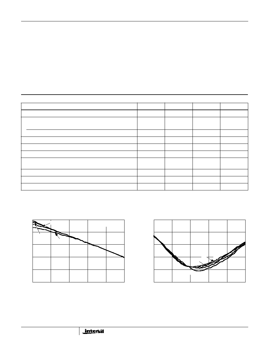
Typical Performance Curves
Power Amplifier Small Signal Performance
NOTE: All data measured at T
A
= 25
o
C and V
G1
, V
G2
and V
G3
adjusted for first stage quies-
cent current of 20mA, second stage current of 53mA and third stage current of 90mA, respectively.
FIGURE 1. LINEAR GAIN
FIGURE 2. INPUT MATCH
6V
2.0
2.2
2.4
2.6
2.8
3.0
35
25
20
15
10
FREQUENCY (GHz)
GAIN (dB)
30
V
DD1
= V
DD2
= V
DD3
5V
3V
4V
6V
2.0
2.2
2.4
2.6
2.8
3.0
-5
-15
-20
-25
-30
FREQUENCY (GHz)
RETURN LOSS (dB)
-10
5V
3V
4V
HFA3926
2-232
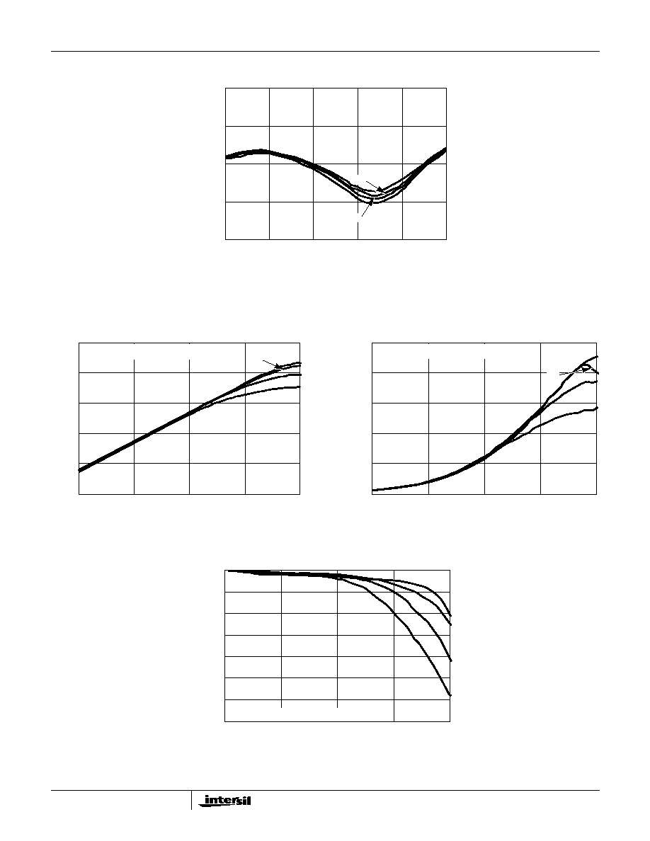
FIGURE 3. OUTPUT MATCH
Power Amplifier CW Performance at Various Supply Voltages
NOTE: All data measured at T
A
= 25
o
C and V
G1
, V
G2
and V
G3
adjusted for first stage quiescent current of 20mA, second stage current of 53mA and third stage current of 90mA, respectively.
FIGURE 4. POWER OUTPUT
FIGURE 5. POWER ADDED EFFICIENCY
FIGURE 6. GAIN COMPRESSION
Typical Performance Curves
(Continued)
6V
2.0
2.2
2.4
2.6
2.8
3.0
0
-5
-10
-15
-20
FREQUENCY (GHz)
RETURN LOSS (dB)
5V
3V
4V
6V
-19
-14
-9
-4
1
30
20
15
10
5
POWER INPUT (dBm)
PO
WER (dBm)
25
2.45GHz, V
DD1
= V
DD2
= V
DD3
5V
3V
4V
6V
-19
-14
-9
-4
1
50
30
20
10
0
INPUT POWER (dBm)
EFFICIENCY (%)
40
5V
3V
4V
2.45GHz, V
DD1
= V
DD2
= V
DD3
6V
0
-2
-3
-4
-7
INPUT POWER (dBm)
COMPRESSION (dBm)
-1
5V
3V
4V
2.45GHz, V
DD1
= V
DD2
= V
DD3
-5
-6
-19
-14
-9
-4
1
HFA3926

2-233
Power Amplifier Temperature Performance
NOTE: All data measured at T
A
= 25
o
C and V
G1
, V
G2
and V
G3
adjusted for first stage quies-
cent current of 20mA, second stage current of 53mA and third stage current of 90mA, respectively.
FIGURE 7. LINEAR GAIN
FIGURE 8. POWER OUTPUT
FIGURE 9. GAIN COMPRESSION
Power Amplifier Spurious Response at Various Supply Voltages
NOTE: All data measured at T
A
= 25
o
C and V
G1
, V
G2
and V
G3
adjusted for first stage quiescent current of 20mA, second stage current of 53mA and third stage current of 90mA, respectively.
FIGURE 10. THIRD ORDER INTERMODULATION RATIO
FIGURE 11. SECOND HARMONIC RATIO
Typical Performance Curves
(Continued)
2.0
2.2
2.4
2.6
2.8
3.0
35
25
20
15
10
FREQUENCY (GHz)
GAIN (dB)
30
25
o
C
70
o
C
V
DD1
= V
DD2
= V
DD3
= +5V
-20
o
C
-19
-14
-9
-4
1
30
20
15
10
0
INPUT POWER (dBm)
PO
WER (dBm)
25
2.45GHz, V
DD1
= V
DD2
= V
DD3
= +5V
5
70
o
C
-20
o
C
25
o
C
0
-2
-3
-4
INPUT POWER (dBm)
COMPRESSION (dB)
-1
-5
-20
-10
-5
0
5
70
o
C
-20
o
C
25
o
C
-15
2.45GHz, V
DD1
= V
DD2
= V
DD3
= +5V
6V
9
13
17
21
25
50
30
20
10
FUNDAMENTAL P
OUT
OF TONES (dBm)
IMR (dBc)
40
2.45GHz, TONE SPACING 600kHz
5V
3V
4V
6V
15
17
19
21
25
70
35
FUNDAMENTAL P
OUT
(dBm)
dBc
40
5V
3V
4V
2.45GHz, V
DD1
= V
DD2
= V
DD3
65
60
55
50
45
23
HFA3926