Äîêóìåíòàöèÿ è îïèñàíèÿ www.docs.chipfind.ru
CAUTION: These devices are sensitive to electrostatic discharge; follow proper IC Handling Procedures.
1-888-INTERSIL or 321-724-7143
|
Intersil (and design) is a registered trademark of Intersil Americas Inc.
Copyright © Intersil Americas Inc. 2002. All Rights Reserved
2-608
®
HFA-0002
Low Noise Wideband
Operational Amplifier
Description
The HFA-0002 is a very wideband, high slew rate, op amp,
featuring precision DC characteristics. Stable in gains of 10
or greater this all bipolar op amp offers a combination of AC
and DC performance never seen before in monolithic form.
The high gain bandwidth product (1GHz) and high slew rate
(250V/
µ
s) make this op amp ideal for use in video and RF
circuits. The low offset voltage (0.6mV), low bias current
(0.23
µ
A), and low voltage noise (2.7nV/
Hz) specifications
combined with the excellent AC characteristics make this op
amp ideal for high speed data acquisition systems with high
accuracy.
Part Number Information
PART
NUMBER
TEMPERA-
TURE RANGE
PACKAGE
HFA2-0002-5
0
o
C to +75
o
C
8 Pin CAN
HFA2-0002-9
-40
o
C to +85
o
C
8 Pin CAN
HFA3-0002-5
0
o
C to +75
o
C
8 Lead Plastic DIP
HFA3-0002-9
-40
o
C to +85
o
C
8 Lead Plastic DIP
HFA7-0002-5
0
o
C to +75
o
C
8 Lead Ceramic Sidebraze DIP
HFA7-0002-9
-40
o
C to +85
o
C
8 Lead Ceramic Sidebraze DIP
HFA9P0002-5
0
o
C to +75
o
C
8 Lead SOIC
HFA9P0002-9
-40
o
C to +85
o
C
8 Lead SOIC
Features
· Wide Gain Bandwidth Product . . . . . . . . . . . . . . . 1GHz
· High Slew Rate . . . . . . . . . . . . . . . . . . . . . . . . . . 250V/
µ
s
· High Open Loop Gain . . . . . . . . . . . . . . . . . . . .105V/mV
· Low Offset Voltage . . . . . . . . . . . . . . . . . . . . . . . . 0.6mV
· Low Power Consumption . . . . . . . . . . . . . . . . . . 143mW
· Low Input Voltage Noise at 1kHz . . . . . . . . . .2.7nV/
Hz
· Monolithic Construction
Applications
· RF/IF Processors
· Video Amplifiers
· Radar Systems
· Pulse Amplifiers
· High Speed Communications
· Fast Data Acquisition Systems
September 1998
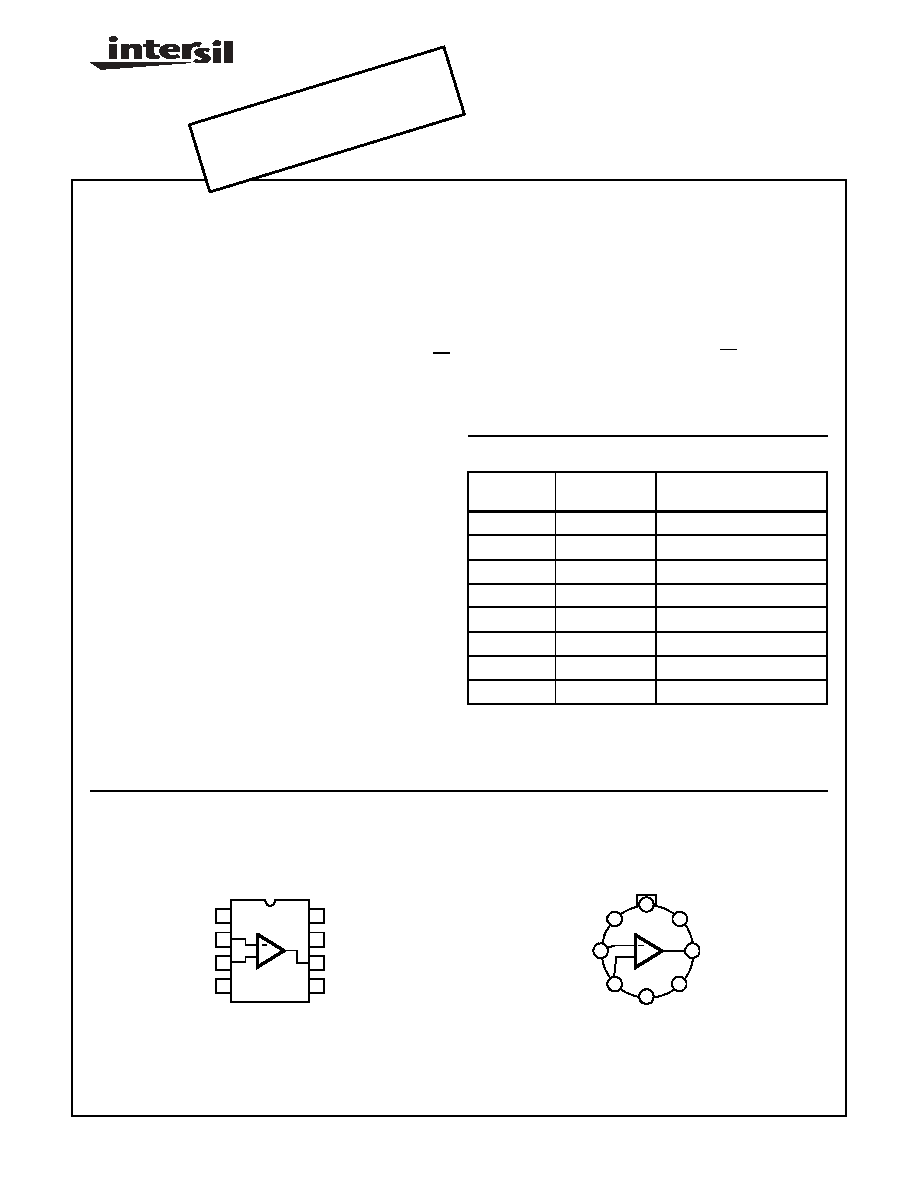
Pinouts
HFA-0002
(PDIP, CDIP, SOIC)
TOP VIEW
HFA-0002
(TO-99 METAL CAN)
TOP VIEW
2
3
4
1
7
6
5
8
+
NC
V+
OUT
BAL
+IN
V-
BAL
IN
-
OUT
BAL
+IN
V+
BAL
2
4
6
1
3
7
5
8
NC
V-
+
IN
-
DB
5
0
0
File Number
2917.3
OBSO
LETE
PRO
DUCT
See H
FA11
00, H
FA11
20, H
FA11
05
or co
ntact
our T
echn
ical S
uppo
rt Ce
nter a
t
1-888
-INTE
RSIL
or w
ww.in
tersil
.com
/tsc
2-609
Specifications HFA-0002
Absolute Maximum Ratings
(Note 1)
Operating Conditions
Supply Voltage Between V+ and V-Terminals . . . . . . . . . . . . . . 12V
Differential Input Voltage . . . . . . . . . . . . . . . . . . . . . . . . . . . . . . . 5V
Input Voltage
. . . . . . . . . . . . . . . . . . . . . . . . . . . . . . . . . . . . . . . . . . . . ±
5V
Output Current
. . . . . . . . . . . . . . . . . . . . . . . . . . . . . . . . . . . . . . . .±
20mA
Junction Temperature (Note 10). . . . . . . . . . . . . . . . . . . . . . +175
o
C
Junction Temperature (Plastic Package) . . . . . . . . . . . . . . . +150
o
C
Lead Temperature (Soldering 10 Sec.) . . . . . . . . . . . . . . . . +300
o
C
Operating Temperature Range :
HFA-0002-9 . . . . . . . . . . . . . . . . . . . . . . . . . . -40
o
C
T
A
+85
o
C
HFA-0002-5 . . . . . . . . . . . . . . . . . . . . . . . . . . . . 0
o
C
T
A
+75
o
C
Storage Temperature Range . . . . . . . . . . . . . . -65
o
C
T
A
150
o
C
CAUTION: Stresses above those listed in "Absolute Maximum Ratings" may cause permanent damage to the device. This is a stress only rating and operation
of the device at these or any other conditions above those indicated in the operational sections of this specification is not implied.
Electrical Specifications
V+ = +5V, V- = -5V, Unless Otherwise Specified
PARAMETER
TEMP
HFA-0002-5/-9
UNITS
MIN
TYP
MAX
INPUT CHARACTERISTICS
Offset Voltage
+25
o
C
-
0.6
1
mV
Full
-
1.2
2
mV
Average Offset Voltage Drift
Full
-
2.0
-
µ
V/
o
C
Bias Current
+25
o
C
-
0.23
1.0
µ
A
High
-
0.1
1.0
µ
A
Low
-
0.32
2.0
µ
A
Offset Current
+25
o
C
-
0.12
1.0
µ
A
Full
-
0.16
1.0
µ
A
Common Mode Range
Full
±
2.5
-
-
V
Differential Input Resistance
+25
o
C
-
1
-
M
Input Capacitance
+25
o
C
-
2
-
pF
Input Noise Voltage
0.1Hz to 10Hz
+25
o
C
-
5.1
-
nV
RMS
10Hz to 1MHz
+25
o
C
-
2.02
-
µ
V
RMS
Input Noise Voltage
f
O
= 10Hz
+25
o
C
-
8.9
-
nV/
Hz
f
O
= 100Hz
+25
o
C
-
3.7
-
nV/
Hz
f
O
= 1000Hz
+25
o
C
-
2.7
-
nV/
Hz
Input Noise Current
f
O
= 10Hz
+25
o
C
-
25
-
pA/
Hz
f
O
= 100Hz
+25
o
C
-
8.4
-
pA/
Hz
f
O
= 1000Hz
+25
o
C
-
4.5
-
pA/
Hz
TRANSFER CHARACTERISTICS
Large Signal Voltage Gain (Note 2, 4)
Full
80
105
-
V/mV
Common Mode Rejection Ratio (Note 3)
+25
o
C
100
110
-
dB
Full
90
108
-
dB
Gain Bandwidth Product
f
O
= 1MHz
+25
o
C
-
1
-
GHz
Minimum Stable Gain
Full
10
-
-
V/V
OUTPUT CHARACTERISTICS
Output Voltage Swing (Note 4)
Full
±
3.5
±
3.9
-
V
Full Power Bandwidth (Note 5)
+25
o
C
10.6
13.3
-
MHz
Output Resistance, Open Loop
+25
o
C
-
5
-
Output Current
Full
±
10
±
12
-
mA
TRANSIENT RESPONSE

2-610
Specifications HFA-0002
Simplified Schematic Diagram
Die Characteristics
Thermal Constants (
o
C/W)
JA
JC
CAN . . . . . . . . . . . . . . . . . . . . . . . . .
117
36
PDIP . . . . . . . . . . . . . . . . . . . . . . . .
96
34
CDIP . . . . . . . . . . . . . . . . . . . . . . . .
75
13
SOIC . . . . . . . . . . . . . . . . . . . . . . . .
158
43
Rise Time (Note 4, 6)
+25
o
C
-
3.2
-
ns
Slew Rate (Note 4, 7, 9)
+25
o
C
200
250
-
V/
µ
s
Settling Time (Note 4, 7)
+25
o
C
-
50
-
ns
Overshoot (Note 4, 6)
+25
o
C
-
30
-
%
POWER SUPPLY CHARACTERISTICS
Supply Current
Full
-
14
20
mA
Power Supply Rejection Ratio (Note 8)
Full
90
99
-
dB
NOTES:
1. Absolute maximum ratings are limiting values, applied individually, beyond which the serviceability of the circuit may be impaired. Func-
tional operation under any of these conditions is not necessarily implied.
2. V
OUT
=
±
3V.
3.
V
CM
=
±
2V.
4. R
L
= 5K, C
L
= 20pF.
5. Full Power Bandwidth is guaranteed by equation: FPBW =
.
6. V
OUT
=
±
100mV, A
V
= +10.
7. V
OUT
=
±
3V, A
V
= +10.
8.
V
S
=
±
4V to
±
6V.
9. This parameter is not tested. This limit is guaranteed based on characterization and reflects lot to lot variation.
10. See Thermal Constants in "Applications Information" section. Maximum power dissipation, including output load, must be designed to
maintain the junction temperature below +175
o
C for hermetic packages, and below +150
o
C for plastic packages.
Electrical Specifications
V+ = +5V, V- = -5V, Unless Otherwise Specified (Continued)
PARAMETER
TEMP
HFA-0002-5/-9
UNITS
MIN
TYP
MAX
Slew Rate
2
Vpeak
------------------------
, Vpeak
3.0V
=
OUT
+V
+IN
+BAL
BAL
IN
V

2-611
HFA-0002
Test Circuits
FIGURE 1. LARGE AND SMALL SIGNAL RESPONSE TEST CIRCUIT
LARGE SIGNAL RESPONSE
Input: 0.2V/Div. Output: 2V/Div.
Horizontal Scale: 20ns/Div.
SMALL SIGNAL RESPONSE
Input: 10mV/Div. Output: 100mV/Div.
FIGURE 3. SETTLING TIME SCHEMATIC
V
OUT
20pF
4.5k
+
500
V
IN
50
0.3V
0V
-0.3V
3V
0V
-3V
IN
OUT
10mV
0V
-10mV
100mV
0V
-100mV
IN
OUT
1K
V
SETTLE
V
OUT
10K
500
5K
+
V
IN
· A
V
= -10
· Feedback and summing resistors must be
matched (0.1%)
· HP5082-2810 clipping diodes recommended
· Tektronix P6201 FET probe used at settling point
2-612
HFA-0002
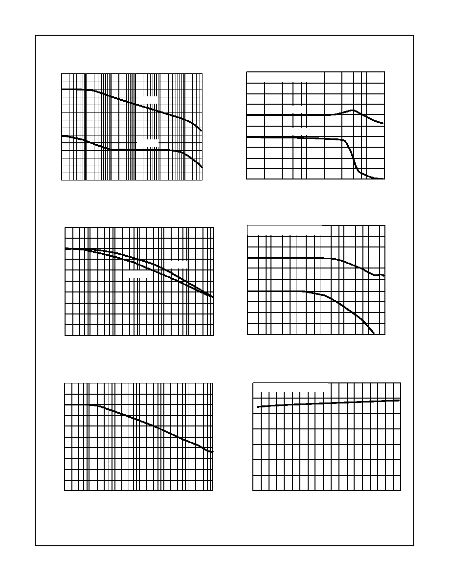
Typical Performance Curves
V
S
=
±
5V, T
A
= +25
o
C, Unless Otherwise Specified
FIGURE 4. OPEN LOOP GAIN AND PHASE vs FREQUENCY
FIGURE 5. CLOSED LOOP GAIN vs FREQUENCY
FIGURE 6. PSRR vs FREQUENCY
FIGURE 7. CLOSED LOOP GAIN vs FREQUENCY
FIGURE 8. CMRR vs FREQUENCY
FIGURE 9. SLEW RATE vs TEMPERATURE
G
A
IN (
d
B)
P
HAS
E
M
ARG
IN (
D
E
G
RE
E
S
)
FREQUENCY (Hz)
120
100
80
60
40
20
0
180
135
90
45
0
1K
10K
100K
1M
10M
100M 500M
PHASE
GAIN
G
A
IN (
d
B)
P
HAS
E
S
H
IF
T
(
D
E
G
RE
E
S
)
80
60
40
20
0
-20
180
135
90
45
0
FREQUENCY (Hz)
1M
10M
100M 200M
GAIN
PHASE
A
V
= +10, R
L
= 5K, C
L
= 20pF
P
S
RR (
d
B)
100
80
60
40
20
0
FREQUENCY (Hz)
1K
10K
100K
1M
10M
100M
100
-PSRR
+PSRR
GA
I
N
(d
B
)
80
60
40
20
0
-20
P
HAS
E
S
H
IF
T
(
D
E
G
RE
E
S
)
180
135
90
45
0
FREQUENCY (Hz)
1K
10K
100K
1M
10M
100M
A
V
= +100, R
L
= 5K, C
L
= 20pF
CM
RR (
d
B)
FREQUENCY (Hz)
1K
10K
100K
1M
10M
100M
100
120
100
80
60
40
20
0
S
L
EW
R
A
T
E (
V
/
µ
s)
TEMPERATURE (
o
C)
300
250
200
150
100
50
0
-60
-40
-20
0
20
40
60
80
100
120
V
OUT
= 3V, R
L
= 5K, C
L
= 20pF
Document Outline