4-1
Semiconductor
[ /Title (HI1176)
/Subject (8-Bit, 20 MSPS, Flash A/D Converter)
/Author ()
/Keywords (Harris Semiconductor, Video, Image Scan-
ner, PC Video capture, Set top box, Clamp, Internal Ref-
erence)
/Creator ()
/DOCINFO pdfmark
[ /PageMode /UseOutlines
/DOCVIEW pdfmark
October 1998
HI1176
8-Bit, 20 MSPS, Flash A/D Converter
Features
∑ Resolution
±
0.5 LSB (DNL) . . . . . . . . . . . . . . . . . . . 8-Bit
∑ Maximum Sampling Frequency . . . . . . . . . . . 20 MSPS
∑ Low Power Consumption at 20 MSPS (Typ)
(Reference Current Excluded) . . . . . . . . . . . . . . .60mW
∑ Built-In Sync Clamp Function
∑ Built-In Monostable Multivibrator for Clamp Pulse
Generation
∑ Built-In Sync Pulse Polarity Selection Function
∑ Clamp Pulse Direct Input Possible
∑ Built-In Clamp ON/OFF Function
∑ Built-In Reference Voltage Self Bias Circuit
∑ Input CMOS Compatible
∑ Three-State TTL Compatible Output
∑ Single +5V Power Supply
∑ Low Input Capacitance (Typ) . . . . . . . . . . . . . . . . 11pF
∑ Reference Impedance (Typ) . . . . . . . . . . . . . . . . . 300
∑ Direct Replacement for the Sony CXD1176
Description
The HI1176 is an 8-bit, CMOS analog-to-digital converter for
video use that features a sync clamp function. The adoption
of a 2-step parallel method realizes low power consumption
and a maximum conversion speed of 20 MSPS. For higher
sampling rates, refer to the pin-for-pin compatible HI1179
data sheet, AnswerFAX document number 3666.
Applications
∑ Video Digitizing
∑ Image Scanners
∑ Low Cost High Speed Data Acquisition Systems
∑ Multimedia
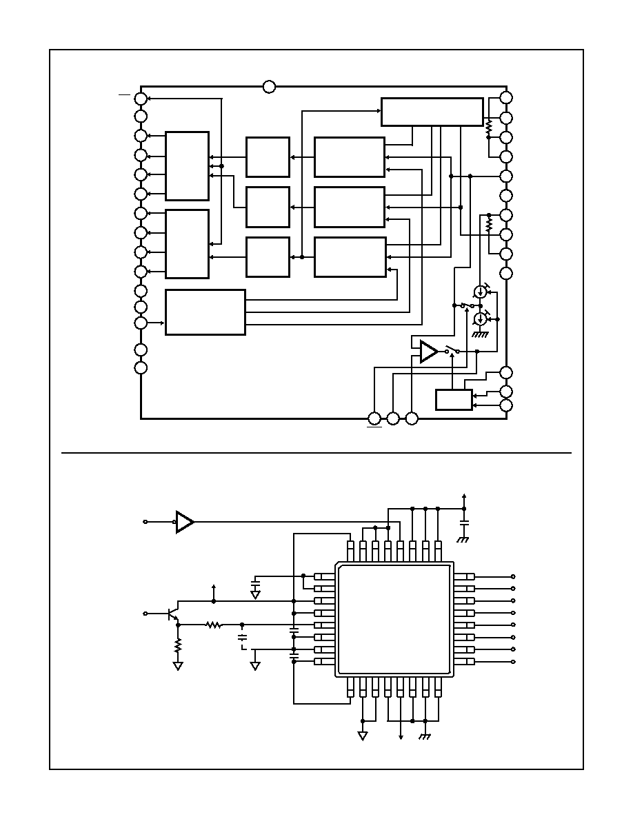
Pinout
HI1176
(MQFP)
TOP VIEW
Ordering Information
PART
NUMBER
TEMP. RANGE
(
o
C)
PACKAGE
PKG. NO.
HI1176JCQ
-40 to 85
32 Ld MQFP
Q32.7x7-S
HI1176-EV
25
Evaluation Board
1
2
3
4
5
6
7
8
(LSB) D0
D1
D2
D3
D4
D5
D6
(MSB) D7
V
RB
AV
SS
AV
SS
V
IN
AV
DD
AV
DD
V
RT
V
RTS
NC
DV
SS
OE
CLE
DV
SS
CCP
V
REF
V
RBS
32 31 30 29 28 27 26 25
24
23
22
21
20
19
18
17
9 10 11 12 13 14 15 16
NC
DV
DD
DV
DD
CLK
SEL
SYNC
PW
AV
DD
CAUTION: These devices are sensitive to electrostatic discharge. Users should follow proper IC Handling Procedures.
Copyright
©
Harris Corporation 1998
File Number
3582.5
NOT RECOMMENDED FOR NEW DESIGNS
See HI1179

4-3
Absolute Maximum Ratings
Thermal Information
Supply Voltage, V
DD
. . . . . . . . . . . . . . . . . . . . . . . . . . . . . . . . . . . 7V
Reference Voltage, V
RT
, V
RB
. . . . . . . . . V
DD
+ 0.5V to V
SS
- 0.5V
Analog Input Voltage, V
IN
. . . . . . . . . . . . . V
DD
+ 0.5V to V
SS
- 0.5V
Digital Input Voltage, CLK. . . . . . . . . . . . . V
DD
+ 0.5V to V
SS
- 0.5V
Digital Output Voltage, V
OH
, V
OL
. . . . . . . V
DD
+ 0.5V to V
SS
- 0.5V
Operating Conditions
(Note 1)
Temperature Range, T
A
. . . . . . . . . . . . . . . . . . . . . . . -40
o
C to 85
o
C
Supply Voltage
AV
DD
, AV
SS
, DV
DD
, DV
SS
. . . . . . . . . . . . . . . +4.75V to +5.25V
|DGND-AGND| . . . . . . . . . . . . . . . . . . . . . . . . . . . .0mV to 100mV
Reference Input Voltage
V
RB
. . . . . . . . . . . . . . . . . . . . . . . . . . . . . . . . . . . . . 0V and Above
V
RT
. . . . . . . . . . . . . . . . . . . . . . . . . . . . . . . . . . . . 2.8V and Below
Analog Input Voltage, V
IN
. . . . . . . . . V
RB
to V
RT
(1.8V
P-P
to AV
DD
)
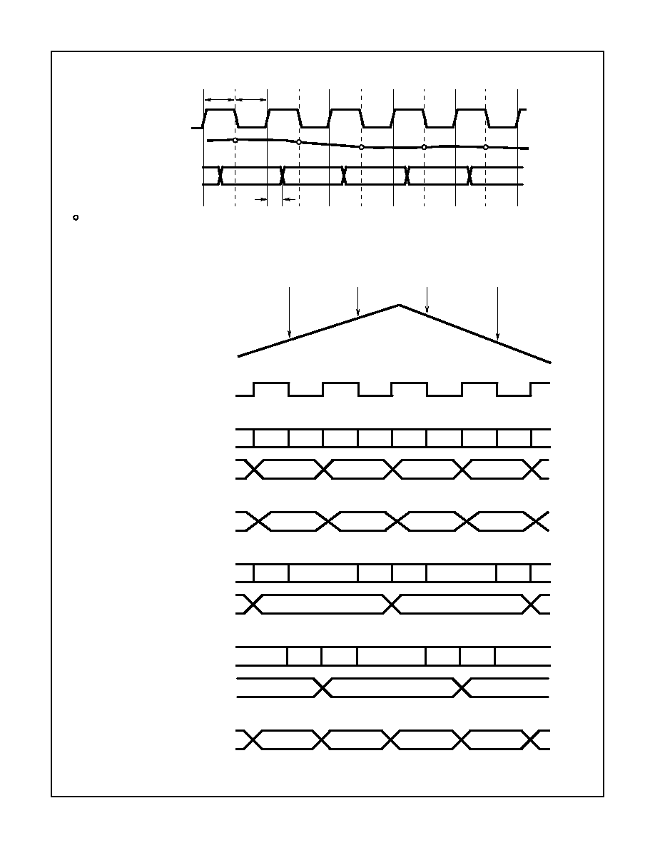
Clock Pulse Width
t
PW1
. . . . . . . . . . . . . . . . . . . . . . . . . . . . . . . . . . . . . . . 25ns (Min)
t
PW0
. . . . . . . . . . . . . . . . . . . . . . . . . . . . . . . . . . . . . . . 25ns (Min)
Thermal Resistance (Typical, Note 1)
JA
(
o
C/W)
MQFP Package . . . . . . . . . . . . . . . . . . . . . . . . . . . .
122
Maximum Junction Temperature . . . . . . . . . . . . . . . . . . . . . . . 150
o
C
Maximum Storage Temperature Range . . . . . . . . . -65
o
C to 150
o
C
Maximum Lead Temperature (Soldering 10s) . . . . . . . . . . . . . 300
o
C
(Lead Tips Only)
CAUTION: Stresses above those listed in "Absolute Maximum Ratings" may cause permanent damage to the device. This is a stress only rating and operation of
the device at these or any other conditions above those indicated in the operational sections of this specification is not implied.
NOTE:
1.
JA
is measured with the component mounted on an evaluation PC board in free air.
Electrical Specifications
f
C
= 20 MSPS, V
DD
= +5V, V
RB
= 0.5V, V
RT
= 2.5V, T
A
= 25
o
C (Note 1)
PARAMETER
TEST CONDITIONS
MIN
TYP
MAX
UNIT
SYSTEM PERFORMANCE
Offset Voltage
E
OT
-60
-40
-20
mV
E
OB
+20
+40
+60
mV
Integral Non-Linearity, INL
f
C
= 20 MSPS, V
IN
= 0.5V to 2.5V
-
±
0.5
±
1.3
LSB
Differential Non-Linearity, DNL
f
C
= 20 MSPS, V
IN
= 0.5V to 2.5V
-
±
0.3
±
0.5
LSB
DYNAMIC CHARACTERISTICS
Signal to Noise Ratio, SINAD
f
S
= 20MHz, f
IN
= 1MHz
-
46
-
dB
f
S
= 20MHz, f
IN
= 3.58MHz
-
46
-
dB
Maximum Conversion Speed, f
C
V
IN
= 0.5V to 2.5V, f
IN
= 1kHz Ramp
20
35
-
MSPS
Minimum Conversion Speed
-
-
0.5
MSPS
Differential Gain Error, DG
NTSC 40 IRE Mod Ramp, f
C
= 14.3 MSPS
-
1.0
-
%
Differential Phase Error, DP
-
0.5
-
Degree
Aperture Jitter, t
AJ
-
30
-
ps
Sampling Delay, t
DS
-
4
-
ns
ANALOG INPUTS
Analog Input Bandwidth (-1dB), BW
-
18
-
MHz
Analog Input Capacitance, C
IN
V
IN
= 1.5V + 0.07V
RMS
-
11
-
pF
RMS Signal
Signal-To -Noise + Distortion Ratio, SINAD
----------------------------------------------------------------------------------------------------------------
HI1176

4-4
REFERENCE INPUT
Reference Pin Current, I
REF
4.5
6.6
8.7
mA
Reference Resistance (V
RT
to V
RB
), R
REF
230
300
450
INTERNAL VOLTAGE REFERENCES
Self Bias
V
RB
Short V
RB
and V
RBS
, Short V
RT
and V
RTS
0.48
0.52
0.56
V
V
RT
- V
RB
1.96
2.08
2.22
V
DIGITAL INPUTS
Digital Input Voltage
V
IH
4.0
-
-
V
V
IL
-
-
1.0
V
Digital Input Current
I
IH
V
DD
= Max
V
IH
= V
DD
-
-
5
µ
A
I
IL
V
IL
= 0V
-
-
5
µ
A
DIGITAL OUTPUTS
Digital Output Current
I
OH
OE = V
SS
, V
DD
= Min
V
OH
= V
DD
-0.5V
-1.1
-
-
mA
I
OL
V
OL
= 0.4V
3.7
-
-
mA
Digital Output Current
I
OZH
OE = V
DD
, V
DD
= Max
V
OH
= V
DD
-
-
16
µ
A
I
OZL
V
OL
= 0V
-
-
16
µ
A
TIMING CHARACTERISTICS
Output Data Delay, t
DL
-
18
30
ns
POWER SUPPLY CHARACTERISTIC
Supply Current, I
DD
f
C
= 20 MSPS, NTSC Ramp Wave Input
-
12
18
mA
CLAMP CHARACTERISTICS
Clamp Offset Voltage, E
OC
V
IN
= DC, PWS = 3
µ
s
V
REF
= 0.5V
0
+20
+40
mV
V
REF
= 2.5V
-50
-30
-10
mV
Clamp Pulse Width (Sync Pin Input), t
CPW
C = 100pF, R = 130k
on Pin 15
1.75
2.75
3.75
µ
s
Clamp Pulse Delay, t
CPD
-
25
-
ns
NOTE:
1. Electrical specifications guaranteed only under the stated operating conditions.
Electrical Specifications
f
C
= 20 MSPS, V
DD
= +5V, V
RB
= 0.5V, V
RT
= 2.5V, T
A
= 25
o
C (Note 1) (Continued)
PARAMETER
TEST CONDITIONS
MIN
TYP
MAX
UNIT
HI1176