3-1
TM
File Number
4114.2
CAUTION: These devices are sensitive to electrostatic discharge; follow proper IC Handling Procedures.
1-888-INTERSIL or 321-724-7143
|
Intersil and Design is a trademark of Intersil Corporation.
|
Copyright
©
Intersil Corporation 2000
HI1177
8-Bit, 40MSPS, 2-Channel D/A Converter
The HI1177 is a dual 8-bit CMOS digital-to-analog converter.
It has input/output equivalent to 2 channels of Y and C for
video use or I and Q for modulators.
The HI1177 is available in the industrial temperature range
and is supplied in a 32 lead plastic metric quad flatpack
(MQFP) package.
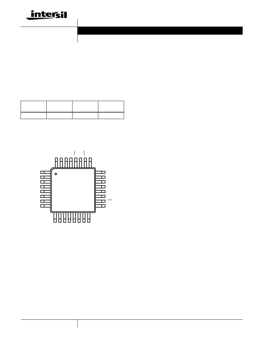
Pinout
HI1177
(MQFP)
TOP VIEW
Features
∑ Resolution . . . . . . . . . . . . . . . . . . . . . . . . . . . . . . . . . 8-Bit
∑ Maximum Conversion Speed . . . . . . . . . . . . . . . . . 40MHz
∑ YC 2-Channel Input/Output
∑ Differential Linearity Error. . . . . . . . . . . . . . . . . .
±
0.3 LSB
∑ Low Power Consumption . . . . . . . . . . . . . . . . . . . .160mW
(200
Load for 2V
P-P
Output)
∑ Power Supply . . . . . . . . . . . . . . . . . . . . . . . . . . +5V Single
∑ Power-Down Mode
∑ Low Glitch Noise
∑ Direct Replacement for Sony CXD1177
Applications
∑ I/Q Modulation
∑ YC Video
∑ Digital TV
∑ Wireless Transmitters
Ordering Information
PART
NUMBER
TEMP.
RANGE (
o
C)
PACKAGE
PKG. NO.
HI1177JCQ
-40 to 85
32 Ld MQFP
Q32.7x7-S
C7
C6
C5
C4
C3
C2
C1
C0
V
REF
CO
CO
Y
O
YO
V
G
AV
DD
DV
DD
Y0
Y1
Y2
Y3
Y4
Y5
Y6
Y7
I
REF
AV
SS
V
B
DV
SS
CCK
YCK
CE
BLK
1
2
3
4
5
6
7
8
16
15
14
13
12
11
10
9
17
18
19
20
21
22
23
24
32 31 30 29 28 27 26 25
Data Sheet
January 1999
3-3
22
V
B
Connect a capacitor of about 0.1
µ
F.
19
YCK
Clock Pin. Moreover all input pins are
TTL-CMOS compatible.
20
CLK
21
DV
SS
Digital GND.
23
AV
SS
Analog GND.
18
CE
Chip Enable Pin. No signal (Output 0V) at "H"
and minimizes power consumption.
24
I
REF
Connect a resistance 16 times "16R" that of
output resistance value "R".
25
V
REF
Set full scale output value.
30
V
G
Connect a capacitor of about 0.1
µ
F.
31
AV
DD
Analog V
DD
.
27
CO
Current Output Pin. Voltage output can be
obtained by connecting a resistance.
29
YO
26
CO
Inverted Current Output Pin. Normally
dropped to analog GND.
28
YO
32
DV
DD
Digital V
DD
.
Pin Descriptions
(Continued)
NUMBER
SYMBOL
EQUIVALENT CIRCUIT
DESCRIPTION
22
DV
SS
DV
DD
DV
DD
19
20
DV
SS
DV
DD
+
-
18
DV
SS
DV
DD
25
AV
SS
AV
DD
AV
DD
24
30
AV
DD
AV
DD
AV
SS
AV
SS
+
-
27
AV
SS
AV
DD
26
AV
SS
AV
DD
29
28
HI1177

3-4
I/O Correspondence Table
(Output Full Scale Voltage: 2V)
Absolute Maximum Ratings
T
A
= 25
o
C
Thermal Information
Supply Voltage, V
DD
. . . . . . . . . . . . . . . . . . . . . . . . . . . . . . . . . . .7V
Input Voltage, V
IN
. . . . . . . . . . . . . . . . . . . . . . . . . . . . . V
DD
to V
SS
Output Current (For Each Channel), l
OUT
. . . . . . . . . . 0mA to 15mA
Operating Conditions
Supply Voltage
AV
DD
, AV
SS
. . . . . . . . . . . . . . . . . . . . . . . . . . . . . . 4.75V to 5.25V
DV
DD
, DV
SS
. . . . . . . . . . . . . . . . . . . . . . . . . . . . . . 4.75V to 5.25V
Reference Input Voltage, V
REF
. . . . . . . . . . . . . . . . . . . . . . . . . 2.0V
Clock Pulse Width
t
PW1
. . . . . . . . . . . . . . . . . . . . . . . . . . . . . . . . . . . . . . 12.5ns (Min)
t
PW0
. . . . . . . . . . . . . . . . . . . . . . . . . . . . . . . . . . . . . . 12.5ns (Min)
Temperature Range, T
OPR
. . . . . . . . . . . . . . . . . . . . -40
o
C to 85
o
C
Thermal Resistance (Typical, Note 7)
JA
(
o
C/W)
MQFP Package . . . . . . . . . . . . . . . . . . . . . . . . . . . .
122
Maximum Junction Temperature (Plastic Package) . . . . . . . .150
o
C
Maximum Storage Temperature Range . . . . . . . . . . -65
o
C to 150
o
C
Maximum Lead Temperature (Soldering 10s) . . . . . . . . . . . . .300
o
C
(MQFP - Lead Tips Only)
CAUTION: Stresses above those listed in "Absolute Maximum Ratings" may cause permanent damage to the device. This is a stress only rating and operation of the
device at these or any other conditions above those indicated in the operational sections of this specification is not implied.
NOTE:
1.
JA
is measured with the component mounted on an evaluation PC board in free air.
Electrical Specifications
f
CLK
= 40MHz, V
DD
= 5V, R
OUT
= 200
, V
REF
= 2.0V, T
A
= 25
o
C
PARAMETER
SYMBOL
TEST CONDITIONS
TEST
LEVEL
OR NOTES
MIN
TYP
MAX
UNITS
Resolution
n
-
8
-
bit
Maximum Conversion Speed
f
MAX
40
-
-
MHz
Linearity Error
E
L
-2.5
-
2.5
LSB
Differential Linearity Error
E
D
-0.3
-
0.3
LSB
Full Scale Output Voltage
V
FS
1.9
2.0
2.2
V
Full Scale Output Ratio
F
SR
Note 1
0
1.5
3
%
Full Scale Output Current
I
FS
-
10
15
mA
Offset Output Voltage
V
OS
-
-
1
mV
Power Supply Current
I
DD
14.3MHz, at Color Bar Data Input
-
-
32
mA
Digital Input
Current
High Level
I
IH
-
-
5
µ
A
Low Level
I
IL
-5
-
-
µ
A
Setup Time
t
S
5
-
-
ns
Hold Time
t
H
10
-
-
ns
Propagation Delay Time
t
PD
-
10
-
ns
Glitch Energy
GE
R
OUT
= 75
-
30
-
pV-s
Cross Talk
CT
1MHz Sin Wave Output
-
57
-
dB
NOTE:
1. Full scale output ratio =
.
INPUT CODE
OUTPUT VOLTAGE
MSB
LSB
1
1
1
1
1
1
1
1
2.0V
∑
∑
∑
1
0
0
0
0
0
0
0
1.0V
∑
∑
∑
0
0
0
0
0
0
0
0
0V
Full-scale voltage of channel
Average of the full-scale voltage of the channels
-------------------------------------------------------------------------------------------------------------------------------
1
≠
( )
x100(%)
HI1177

