10-1
Semiconductor
August 1997
HI1260
Triple 8-Bit, 35 MSPS, RGB,
3-Channel D/A Converter
Features
∑ Resolution . . . . . . . . . . . . . . . . . . . . . . . . . . . Triple 8-Bit
∑ Maximum Conversion Speed . . . . . . . . . . . . . . . 35MHz
∑ RGB 3-Channel Input/Output
∑ Differential Linearity Error . . . . . . . . . . . . . . .
±
0.5 LSB
∑ Digital Input Voltage . . . . . . . . . . . . . . . . . . . .TTL Level
∑ Output Voltage Full Scale (Typ) . . . . . . . . . . . . . . 1V
P-P
∑ Low Power Consumption (Typ) . . . . . . . . . . . . .360mW
∑ Direct Replacement for Sony CXA1260
Applications
∑ Digital TV
∑ Graphics Display
∑ High Resolution Color Graphics
∑ Video Reconstruction
∑ Instrumentation
∑ Image Processing
∑ I/Q Modulation
Description
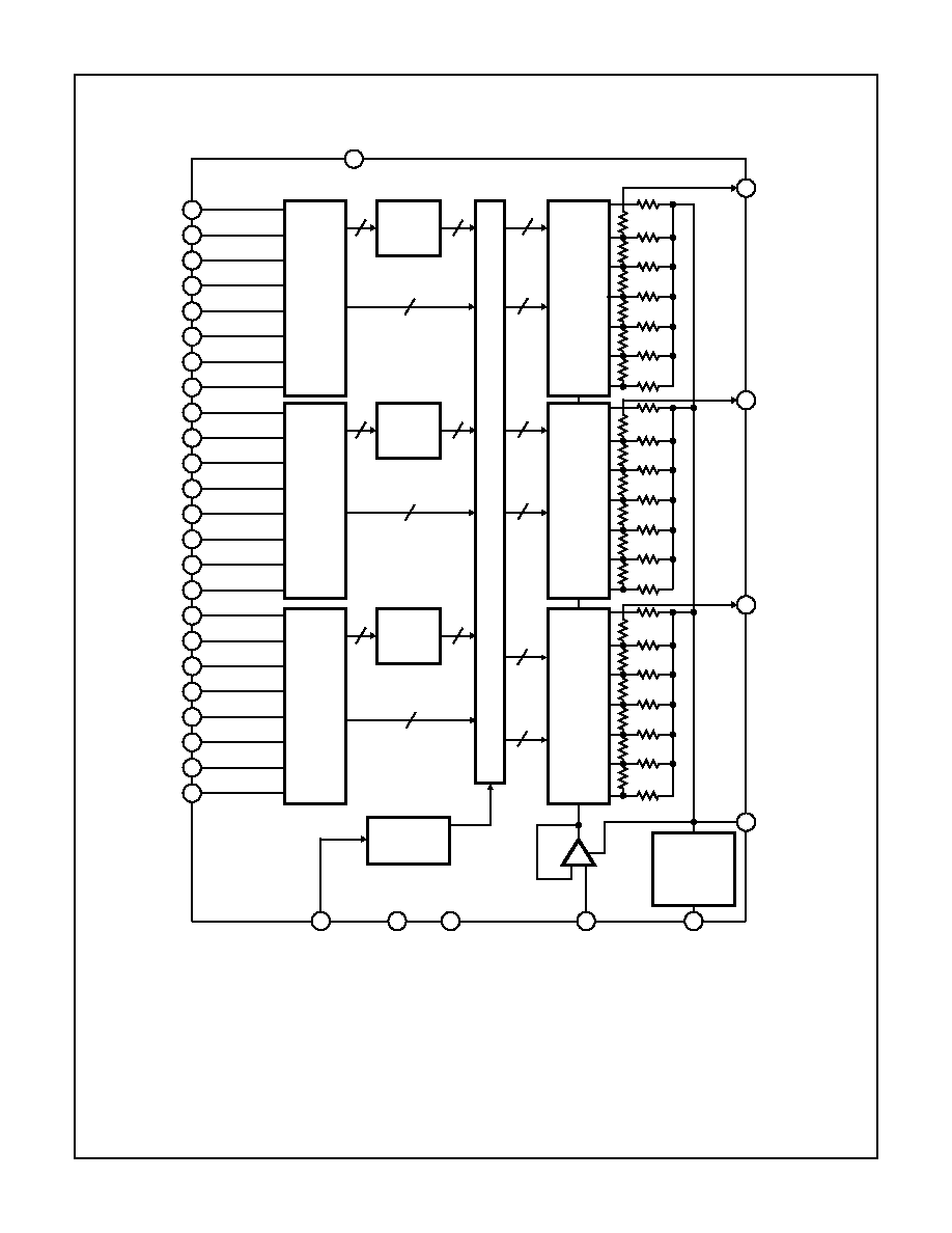
The HI1260 is a triple 8-bit, high-speed, bipolar D/A
converter designed for video band use. It has three sepa-
rate, 8-bit pixel inputs, one each for red, green, and blue
video data. A single 5.0V power supply and pixel clock input
is all that is required to make the device operational. A bias
voltage generator is internal. For lower CMOS power
consumption, refer to the HI1178.
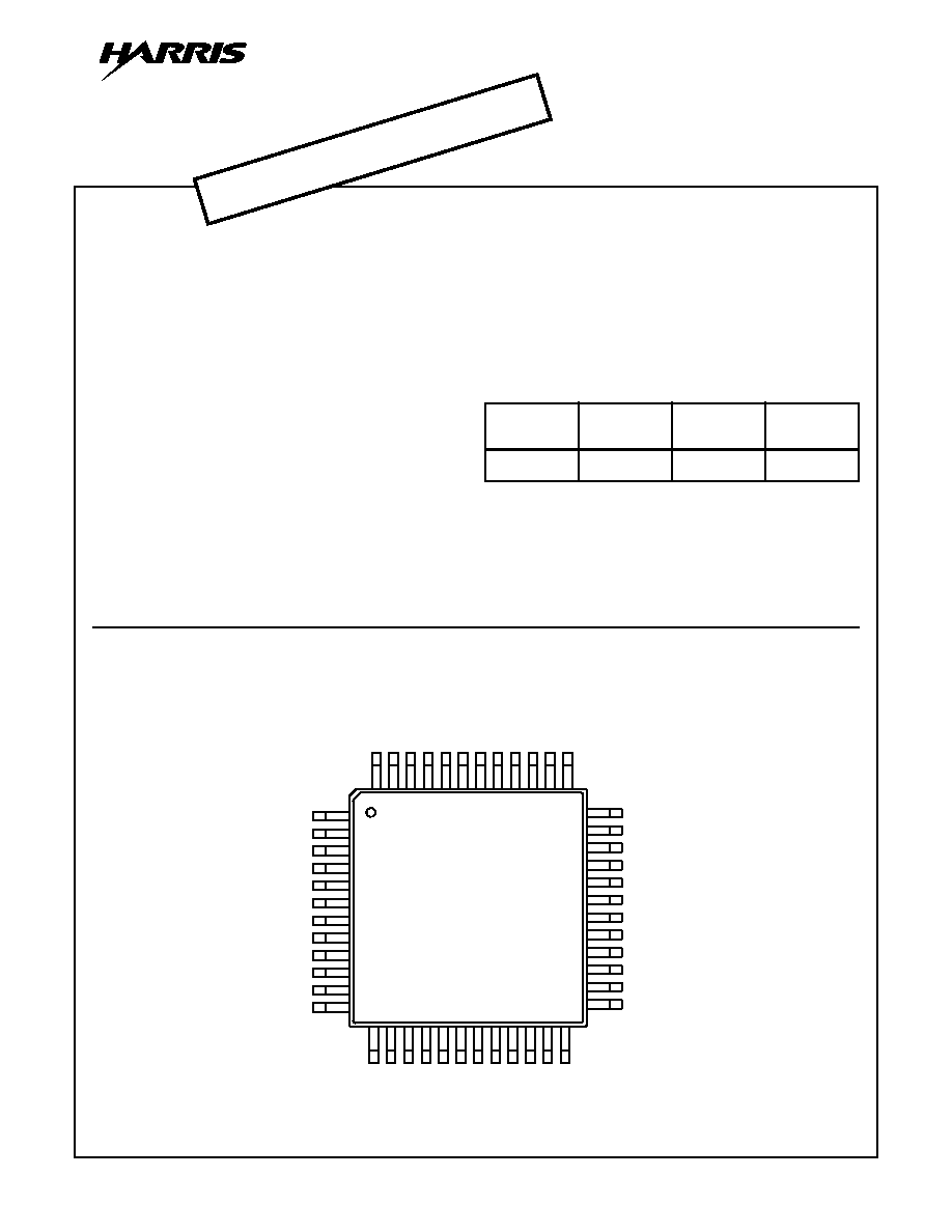
Pinout
HI1260
(MQFP)
TOP VIEW
Ordering Information
PART
NUMBER
TEMP.
RANGE (
o
C)
PACKAGE
PKG. NO.
HI1260JCQ
-20 to 75
48 Ld MQFP
Q48.12 x 12-S
1
2
3
4
5
6
7
8
32
31
30
29
28
27
26
25
24
23
22
21
20
19
18
17
9
10
11
12
13 14 15 16
33
34
35
36
37
38
39
40
41
42
43
44
45
46
47
48
NC
NC
NC
ROUT
NC
GOUT
NC
BOUT
NC
AV
CC
NC
V
REF
G1
G2
G3
G4
G5
G8
B1
B2
B3
B4
G6
G7
NC
R8
R7
R6
R5
R4
R3
R2
R1
NC
DGND
DGND
B5
B6
B7
B8
NC
CLK
DGND
DV
CC
NC
NC
A
GND
V
SET
CAUTION: These devices are sensitive to electrostatic discharge. Users should follow proper IC Handling Procedures.
Copyright
©
Harris Corporation 1997
File Number
4112.1
NOT RECOMMENDED FOR NEW DESIGNS
See HI1178
10-4
26
NC
Vacant pin (no connection).
27
AV
CC
Analog V
CC
.
28
NC
Vacant pin but connect to AV
CC
(Note 1).
29
B
OUT
Analog Output pin for BLUE.
30
NC
Vacant pin but connect to AV
CC
(Note 1).
31
G
OUT
Analog Output pin for GREEN.
32
NC
Vacant pin but connect to AV
CC
(Note 1).
33
R
OUT
Analog Output pin for RED.
34 To 36
NC
Vacant pin but connect to AV
CC
(Note 1).
19, 37, 43
DGND
Digital GND.
48
NC
Vacant pin (no connection).
NOTE:
1. Pins 30, 32, 34 and 36 are vacant, but in order to reduce interference between the individual RGB outputs, connect them to AV
CC
.
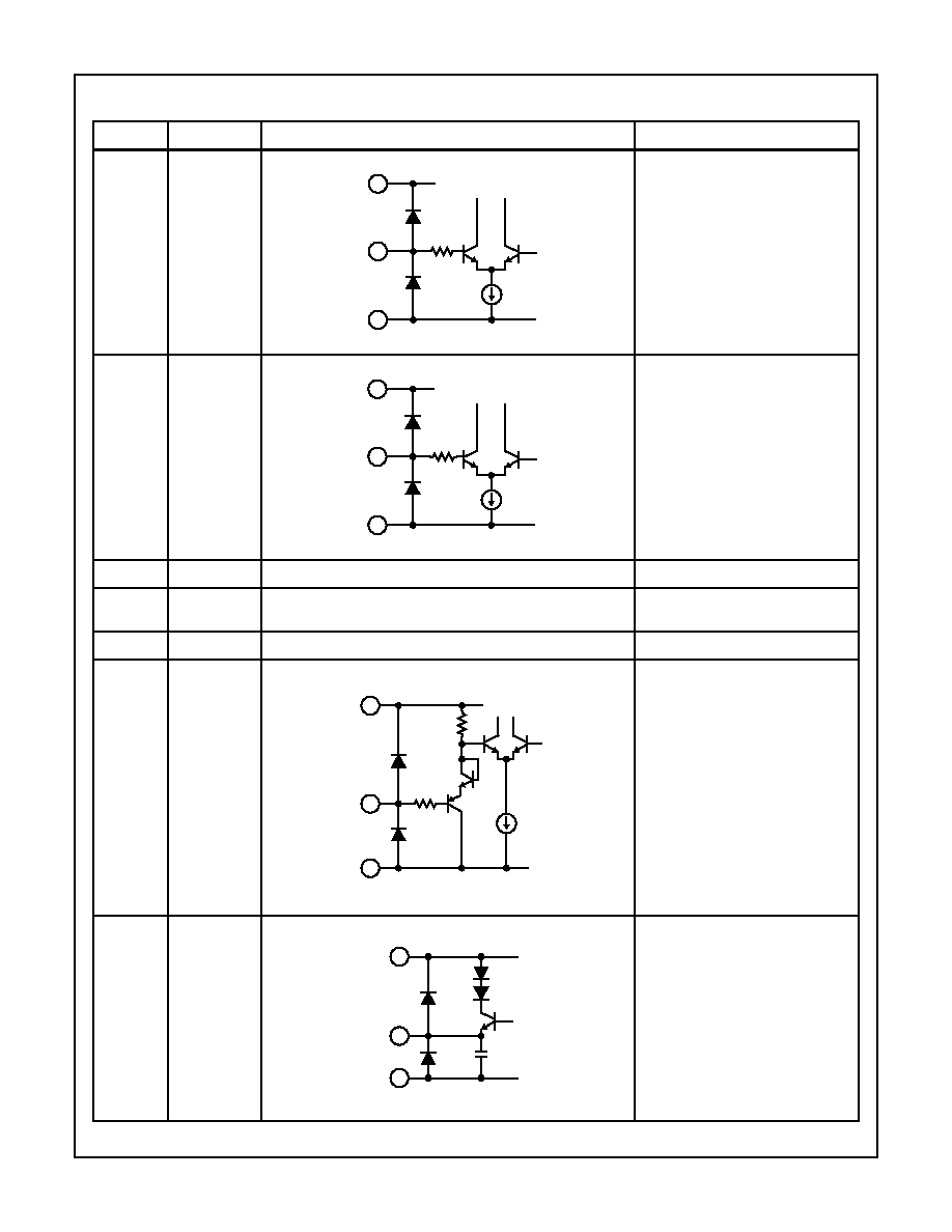
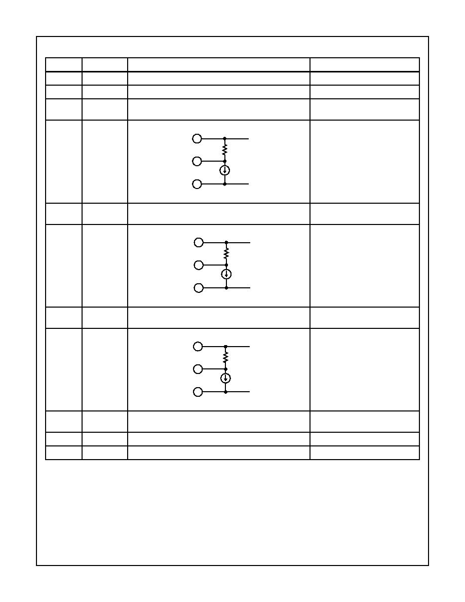
Pin Descriptions
(Continued)
NUMBER
SYMBOL
EQUIVALENT CIRCUIT
DESCRIPTION
R
O
AGND
AV
CC
27
29
23
R
O
AGND
AV
CC
27
31
23
R
O
AGND
AV
CC
27
33
23
HI1260
10-5
Absolute Maximum Ratings
T
A
= 25
o
C
Thermal Information
Supply Voltage, V
CC
. . . . . . . . . . . . . . . . . . . . . . . . . . . . . . .0V to 7V
Input Voltage (Digital)
V
I
. . . . . . . . . . . . . . . . . . . . . . . . . . . . . . . . . . . . . . . . -0.3V to V
CC
V
CLK
. . . . . . . . . . . . . . . . . . . . . . . . . . . . . . . . . . . . . -0.3V to V
CC
Input Voltage (V
SET
Pin), V
SET
. . . . . . . . . . . . . . . . . . -0.3V to V
CC
Output Voltage (Analog), V
OUT
. . . . . . . . . . . . . . V
CC
-2.1V to V
CC
Output Current (Analog), I
OUT
. . . . . . . . . . . . . . . . . . -3mA to 10mA
(V
REF
Pin), I
REF
. . . . . . . . . . . . . . . . . . . . . . . . . . . . -5mA to 0mA
Allowable Power Dissipation, P
D
. . . . . . . . . . . . . . . . . . . . . . . 0.7W
Thermal Resistance (Typical, Note 2)
JA
(
o
C/W)
MQFP Package . . . . . . . . . . . . . . . . . . . . . . . . . . . .
85
Maximum Junction Temperature (Plastic Package) . . . . . . . . 150
o
C
Maximum Storage Temperature Range . . . . . . . . . .-55
o
C to 150
o
C
Maximum Lead Temperature (Soldering 10s) . . . . . . . . . . . . . 300
o
C
(Lead Tips Only)
Recommended Operating Conditions
Temperature Range . . . . . . . . . . . . . . . . . . . . . . . . . -20
o
C to 75
o
C
Supply Voltage
AV
CC
, DV
CC
. . . . . . . . . . . . . . . . . . . . . . . . . . . . . . . .4.5V to 5.5V
AV
CC
- DV
CC
. . . . . . . . . . . . . . . . . . . . . . . . . . . . . . -0.2V to 0.2V
AGND - DGND . . . . . . . . . . . . . . . . . . . . . . . . . . -0.05V to 0.0.5V
Digital Input Voltage
H Level, V
IH
, V
CLKH
. . . . . . . . . . . . . . . . . . . . . . . . .2.0V to DV
CC
L Level, V
IL
, V
CLKL
. . . . . . . . . . . . . . . . . . . . . . . . . DGND to 0.8V
V
SET
Input Voltage, V
SET
. . . . . . . . . . . . . . . . . . . . . . . 0.7V to 1.0V
V
REF
Pin Current, I
REF
. . . . . . . . . . . . . . . . . . . . . . . -3mA to 0.4mA
Clock Pule Width
t
PW1
. . . . . . . . . . . . . . . . . . . . . . . . . . . . . . . . . . . . . . . . . . . . 15ns
t
PW0
. . . . . . . . . . . . . . . . . . . . . . . . . . . . . . . . . . . . . . . . . . . . 10ns
CAUTION: Stresses above those listed in "Absolute Maximum Ratings" may cause permanent damage to the device. This is a stress only rating and operation
of the device at these or any other conditions above those indicated in the operational sections of this specification is not implied.
NOTE:
2.
JA
is measured with the component mounted on an evaluation PC board in free air.
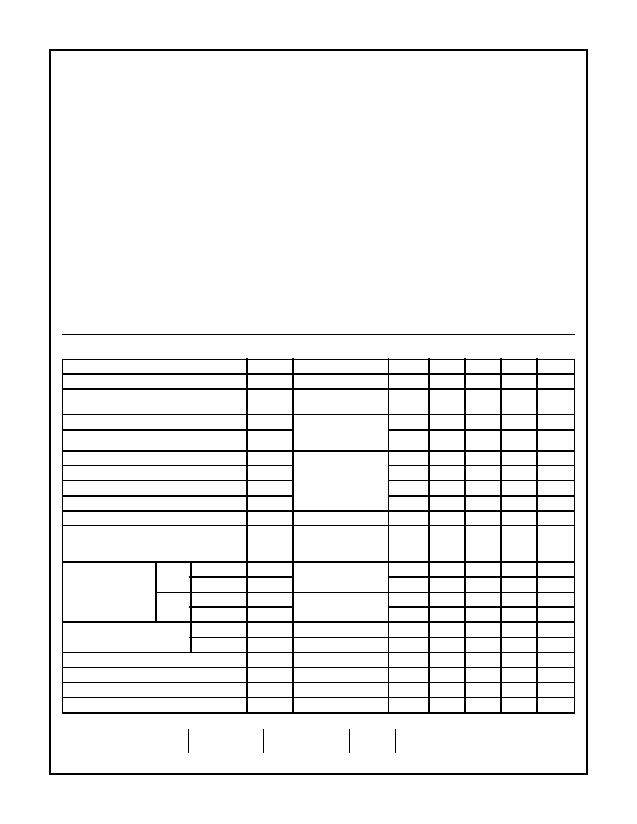
Electrical Specifications
T
A
= 25
o
C, AV
CC
= DV
CC
= 5.0V, AGND = DGND = 0.0V
PARAMETER
SYMBOL
TEST CONDITIONS
NOTES
MIN
TYP
MAX
UNITS
Resolution
RSL
-
8
-
Bit
Monotony
MNT
-
Guar-
antee
-
-
Differential Linearity Error
DLE
V
SET
- AGND = 0.87V
R
L
> 10k
FS = Full Scale
-0.5
-
0.5
LSB
Integral Linearity Error
ILE
-0.4
-
4
% of FS
Maximum Conversion Speed
f
MAX
V
SET
- AGND = 0.87V
R
L
> 10k
C
L
< 20pF
35
-
-
MSPS
Full Scale Output Voltage
V
OFS
Note 3
0.85
1.0
1.15
V
P-P
RGB Output Voltage Full Scale Ratio
FSR
Note 4
0
4
8
%
Output Zero Offset Voltage
V
OFFSET
-40
-6
0
mV
Output Resistance
R
O
270
340
420
Consumption Current
I
D
V
SET
- AGND = 0.87V
R
L
> 10k
I
REF
= -400
µ
A
54
72
90
mA
Digital Data Input
Current
H
Level
Upper 2 Bits
I
IH(U)
V
I
= DV
CC
-
1.2
20
µ
A
Lower 6 Bits
I
IH(L)
-
0.6
10
µ
A
L
Level
Upper 2 Bits
I
IL(U)
V
I
= DGND
-10
0
10
µ
A
Lower 6 Bits
I
IL(L)
-10
0
10
µ
A
Clock Input Current
H Level
I
CLKH
V
CLK
= DV
CC
-
3
30
µ
A
L Level
I
CLKL
V
CLK
= DGND
-10
0
10
µ
A
V
SET
Input Current
I
SET
V
SET
= AGND = 0.87V
-5
-0.3
0
µ
A
Internal Reference Voltage
V
REF
I
REF
= -400
µ
A
1.08
1.20
1.32
V
Set-Up Time
t
S
12
-
-
ns
Hold Time
t
H
3
-
-
ns
NOTES:
3. AV
CC
- V
0
.
4. Maximum value among
.
100
V
O FS R
( )
V
O FS G
( )
------------------------
1
≠
◊
,100
V
O FS G
( )
V
O FS B
( )
------------------------
1
≠
◊
, or 100
V
O FS B
( )
V
O FS R
( )
------------------------
1
≠
◊
HI1260