4-1148
August 1997
HI1386
8-Bit, 75 MSPS, Flash A/D Converter
Features
∑ Differential Linearity Error
±
0.5 LSB or Less
∑ Integral Linearity Error
±
0.5 LSB or Less
∑ Built-In Integral Linearity Compensation Circuit
∑ High-Speed Operation with Maximum Conversion
Rate (Min) . . . . . . . . . . . . . . . . . . . . . . . . . . . . . 75 MSPS
∑ Low Input Capacitance (Typ) . . . . . . . . . . . . . . . . . 17pF
∑ Wide Analog Input Bandwidth
(Min for Full Scale Input) . . . . . . . . . . . . . . . . . . 150MHz
∑ Single Power Supply . . . . . . . . . . . . . . . . . . . . . . . -5.2V
∑ Low Power Consumption (Typ) . . . . . . . . . . . . .580mW
∑ Low Error Rate
∑ Operable at 50% Clock Duty Cycle
∑ Capable of Driving 50
Loads
∑ Direct Replacement for CXA1386
Applications
∑ Video Digitizing
∑ RGB Graphics Processing
∑ HDTV (High Definition TV)
∑ Radar Systems
∑ Communication Systems
∑ Direct RF Down-Conversion
∑ Digital Oscilloscopes
Description
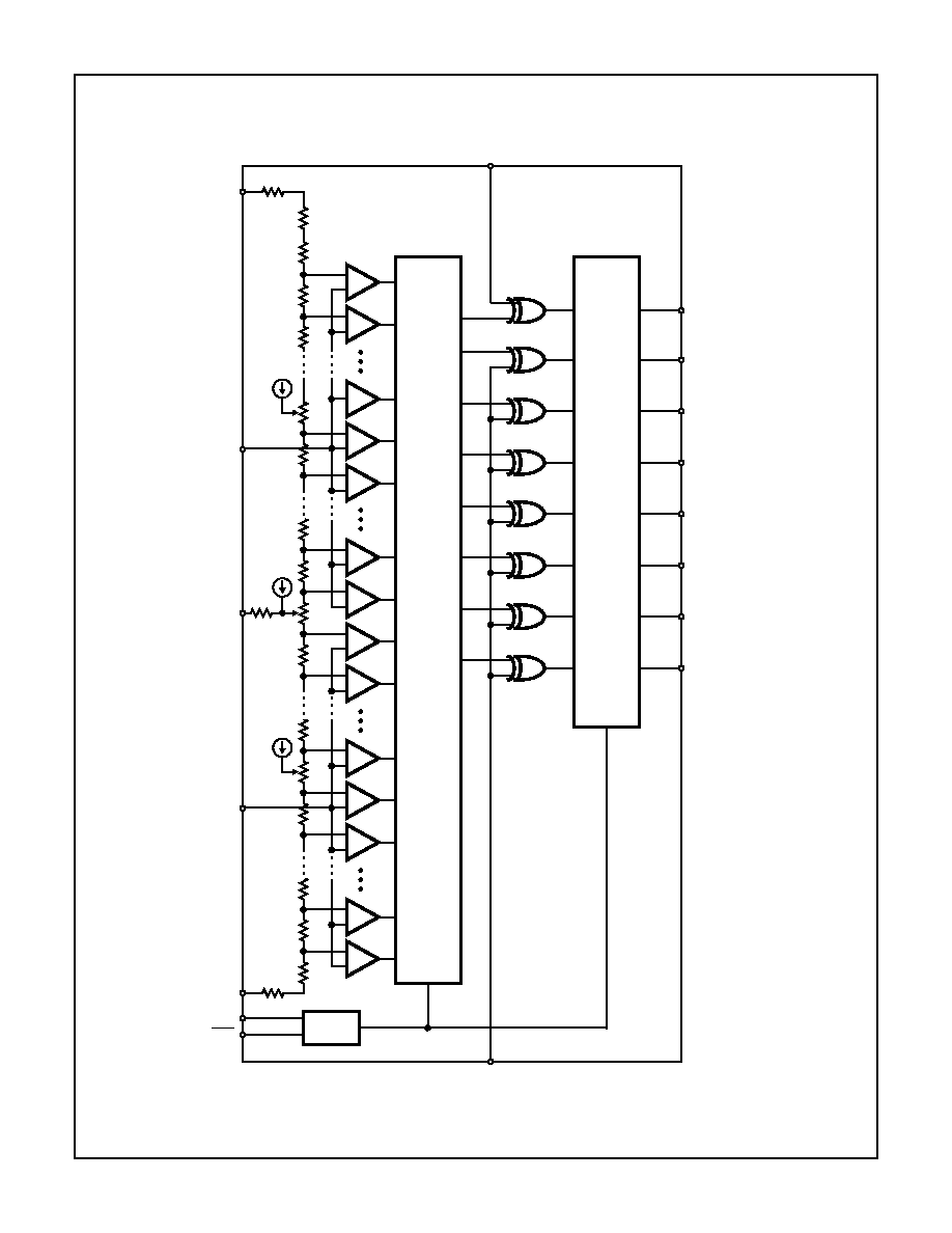
The HI1386 is an 8-bit, high-speed flash analog-to-digital
converter IC capable of digitizing analog signals at a
maximum rate of 75 MSPS. The digital I/O levels of this A/D
converter are compatible with ECL 100K/10KH/10K.
The HI1386 is available in the commercial and industrial
temperature range and is supplied in 28 lead plastic DIP and
44 lead ceramic LCC packages.
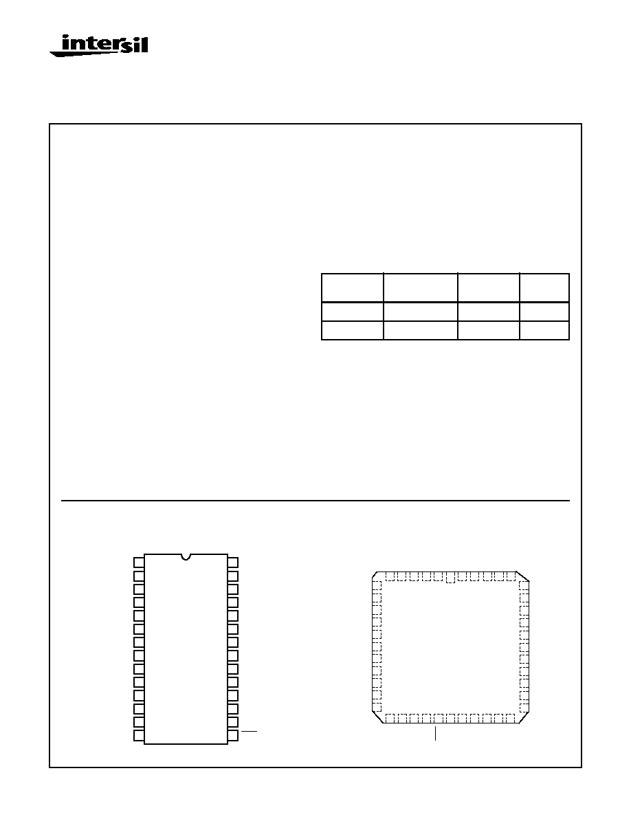
Pinouts
HI1386 (PDIP)
TOP VIEW
HI1386 (CLCC)
TOP VIEW
Ordering Information
PART
NUMBER
TEMP.
RANGE (
o
C)
PACKAGE
PKG. NO.
HI1386JCP
-20 to 75
28 Ld PDIP
E28.6A-S
HI1386AIL
-20 to 100
44 Ld CLCC
J44.B
28
27
26
25
24
23
22
21
20
19
18
17
16
15
LINV
DV
EE
DGND
(LSB) D0
D1
D2
D3
D4
D5
D6
(MSB) D7
DGND
DV
EE
MINV
1
2
3
4
5
6
7
8
9
10
11
12
13
14
AV
EE
AV
EE
AGND
V
IN
AGND
AGND
AGND
AV
EE
V
RB
CLK
CLK
V
RT
V
RM
V
IN
D5
DGND2
NC
(LSB) D0
D6
D4
NC
NC
DGND1
DV
EE
MINV
CLK
CLK
V
RB
AV
EE
NC
AV
EE
NC
D2
D3
(MSB) D7
D1
14
13
12
11
10
9
8
7
17
16
15
2
5
30
35
39
38
37
36
33
34
32
31
29
4
6
3
1
40
41
42
43
44
28
27
26
25
24
23
22
21
20
19
18
DGND2
DGND1
AV
EE
NC
V
RT
DV
EE
AV
EE
AV
EE
LINV
NC
NC
NC
NC
AGND
V
IN
AGND
V
RM
AGND
V
IN
AGND
NC
NC
File Number
3583.4
CAUTION: These devices are sensitive to electrostatic discharge; follow proper IC Handling Procedures.
http://www.intersil.com or 407-727-9207
|
Copyright
©
Intersil Corporation 1999
4-1150
Pin Descriptions
PIN NUMBER
SYMBOL
I/O
STANDARD
VOLTAGE
LEVEL
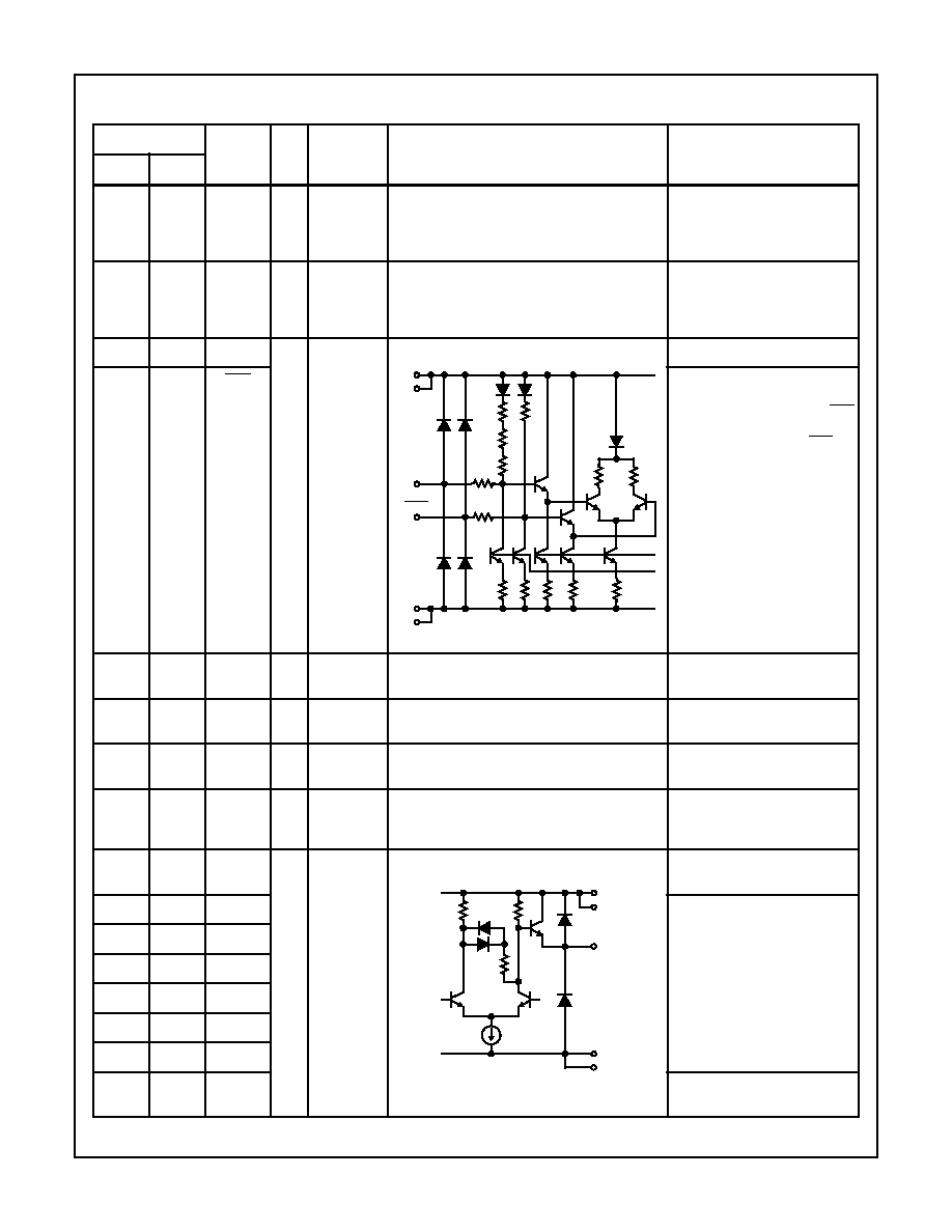
EQUIVALENT CIRCUIT
DESCRIPTION
DIP
LCC
19, 21,
23, 25
31, 33,
35, 37
AGND
-
0V
Analog GND. Used as GND for
input buffers and latches of
comparators. Isolated from DGND,
DGND1, and DGND2.
18, 26,
28
27, 28,
40, 41,
44
AV
EE
-
-5.2V
Analog V
EE
-5.2V (Typ). Internally
connected to DV
EE
(Resistance:
4
to 6
). Bypass with 0.1
µ
F to
AGND.
16
23
CLK
I
ECL
CLK Input.
15
22
CLK
Input Complementary to CLK.
When open pulled down to -1.3V.
Device is operable without CLK
input, but use of complementary
inputs of CLK and
CLK is
recommended to obtain stable
high speed operation.
3, 12
-
DGND
-
0V
Digital GND (used for internal
circuits and output transistors).
-
5, 19
DGND1
-
0V
Digital GND (used for internal
circuits and output transistors).
-
6,
16
DGND2
-
0V
Digital GND (used for output
buffers).
2, 13
4, 20
DV
EE
-
-5.2V
Digital V
EE
. Internally connected
to AV
EE
(resistance: 4
to 6
).
Bypass with 0.1
µ
F to DGND
4
8
D0
O
ECL
LSB of Data Outputs. External
pull-down resistor is required.
5
9
D1
Data Outputs. External pull-down
resistors are required.
6
10
D2
7
11
D3
8
12
D4
9
13
D5
10
14
D6
11
15
D7
MSB of Data Outputs. External
pull-down resistor is required.
DV
EE
CLK
CLK
DGND, DGND1
R
R
R
R
R
R
DV
EE
DGND
D1
HI1386
4-1151
1
3
LINV
I
ECL
Input Pin for D0 (LSB) to D6
Output Polarity Inversion (see A/D
Output Code Table). Pulled low
when left open.
14
21
MINV
I
ECL
Input Pin for D7 (MSB) Output
Polarity Inversion (see A/D Output
Code Table). Pulled low when left
open.
20, 24
32, 36
V
IN
I
V
RT
to V
RB
Analog Input Pins. These two pins
must be connected externally,
since they are not internally
connected. See Application Note
for precautions.
17
26
V
RB
I
-2V
Reference Voltage (Bottom).
Typically -2V. Bypass with a
0.1
µ
F and 10
µ
F to AGND.
22
34
V
RM
I
V
RB
/2
Reference Voltage Mid Point.
Can be used as a pin for integral
linearity compensation.
27
42
V
RT
I
0V
Reference Voltage (Top) Typically
0V.
Pin Descriptions
(Continued)
PIN NUMBER
SYMBOL
I/O
STANDARD
VOLTAGE
LEVEL
EQUIVALENT CIRCUIT
DESCRIPTION
DIP
LCC
R
R
R
R
-1.3V
DV
EE
DGND, DGND1
LINV
OR
MINV
V
IN
V
IN
AV
EE
AGND
R
R
V
RT
R/2
R1
COMPARATOR 1
COMPARATOR 127
R
COMPARATOR 128
R2
V
RM
R
COMPARATOR 129
R
COMPARATOR 130
COMPARATOR 255
R/2
V
RB
R3
COMPARATOR 2
R
R
HI1386
4-1152
Absolute Maximum Ratings
T
A
= 25
o
C
Thermal Information
Supply Voltage (AV
EE
, DV
EE
) . . . . . . . . . . . . . . . . . . . -7V to +0.5V
Analog Input Voltage (V
IN
) . . . . . . . . . . . . . . . . . . . . . -2.7V to +0.5V
Reference Input Voltage
V
RT
, V
RB
, V
RM
. . . . . . . . . . . . . . . . . . . . . . . . . . . -2.7V to +0.5V
|V
RT
-V
RB
| . . . . . . . . . . . . . . . . . . . . . . . . . . . . . . . . . . . . . . . 2.5V
Digital Input Voltage
CLK, CLK, MINV, LINV . . . . . . . . . . . . . . . . . . . . . . . -4V to +0.5V
|CLK-CLK | . . . . . . . . . . . . . . . . . . . . . . . . . . . . . . . . . . . . . . . 2.7V
V
RM
Pin Input Current (I
VRM
) . . . . . . . . . . . . . . . . . . -3mA to +3mA
Digital Output Current (ID0 to ID7) . . . . . . . . . . . . . . . -30mA to 0mA
Thermal Resistance (Typical, Note 1)
JA
o
C/W
JC
o
C/W
PDIP Package . . . . . . . . . . . . . . . . . . .
58
N/A
CLCC Package . . . . . . . . . . . . . . . . . .
45
11
Maximum Junction Temperature
CLCC Package . . . . . . . . . . . . . . . . . . . . . . . . . . . . . . . . . . 175
o
C
PDIP Package . . . . . . . . . . . . . . . . . . . . . . . . . . . . . . . . . . . 150
o
C
Maximum Storage Temperature Range (T
STG
) . . . .-65
o
C to 150
o
C
Maximum Lead Temperature (Soldering 10s) . . . . . . . . . . . . 300
o
C
Operating Conditions
Temperature Ranges (Note 4)
PDIP Package (T
A
) . . . . . . . . . . . . . . . . . . . . . . . . . -20
o
C to 75
o
C
CLCC Package (T
C
) . . . . . . . . . . . . . . . . . . . . . . . -20
o
C to100
o
C
Supply Voltage
AV
EE
, DV
EE
. . . . . . . . . . . . . . . . . . . . . . . . . . . . . -5.5V to -4.95V
AV
EE
- DV
EE
. . . . . . . . . . . . . . . . . . . . . . . . . . . . . -0.05V to 0.05V
AGND - DGND . . . . . . . . . . . . . . . . . . . . . . . . . . . -0.05V to 0.05V
Reference Input Voltage
V
RT
. . . . . . . . . . . . . . . . . . . . . . . . . . . . . . . . . . . . . . -0.1V to 0.1V
V
RB
. . . . . . . . . . . . . . . . . . . . . . . . . . . . . . . . . . . . . -2.2V to -1.8V
Analog Input Voltage, V
IN
. . . . . . . . . . . . . . . . . . . . . . . . V
RB
to V
RT
Pulse Width of Clock
t
PW1
. . . . . . . . . . . . . . . . . . . . . . . . . . . . . . . . . . . . . . . 6.6ns (Min)
t
PW0
. . . . . . . . . . . . . . . . . . . . . . . . . . . . . . . . . . . . . . . 6.6ns (Min)
CAUTION: Stresses above those listed in "Absolute Maximum Ratings" may cause permanent damage to the device. This is a stress only rating and operation of
the device at these or any other conditions above those indicated in the operational sections of this specification is not implied.
NOTE:
1.
JA
is measured with the component mounted on an evaluation PC board in free air.
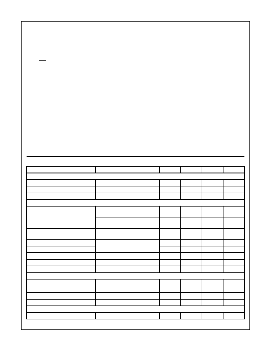
Electrical Specifications
T
A
= 25
o
C, AV
EE
= DV
EE
= -5.2V, V
RT
= 0V, V
RB
= -2V (Note 1)
PARAMETER
TEST CONDITIONS
MIN
TYP
MAX
UNIT
SYSTEM PERFORMANCE
Resolution
-
8
-
Bits
Integral Linearity Error, INL
f
C
= 75MHz
-
±
0.3
±
0.5
LSB
Differential Linearity Error, DNL
f
C
= 75MHz
-
±
0.3
±
0.5
LSB
DYNAMIC CHARACTERISTICS
Signal to Noise and Distortion Ratio, SINAD
Input = 1MHz, Full Scale
f
C
= 75MHz
-
46
-
dB
Input = 18.75MHz, Full Scale
f
C
= 75MHz
-
40
-
dB
Error Rate
Input = 18.749MHz, Full Scale
Error > 16 LSB, f
C
= 75MHz
-
-
10
-9
TPS
(Note 2)
Differential Gain Error, DG
NTSC 40 IRE Mod. Ramp,
f
C
= 75 MSPS
-
1.0
-
%
Differential Phase Error, DP
-
0.5
-
Degree
Maximum Conversion Rate, f
C
Error Rate of 10
-9
TPS (Note 2)
75
-
-
MSPS
Aperture Jitter, t
AJ
-
10
-
ps
Sampling Delay, t
DS
-
3.0
-
ns
ANALOG INPUT
Input Bandwidth
V
IN
= 2V
P-P
(-3dB)
150
-
-
MHz
Analog Input Capacitance, C
IN
V
IN
= 1V + 0.07V
RMS
-
17
-
pF
Analog Input Resistance, R
IN
-
390
-
k
Input Bias Current, I
IN
V
IN
= -1V
-
-
200
µ
A
REFERENCE INPUTS
Reference Resistance, R
REF
75
110
155
RMS Signal
RMS Noise
Distor tion
+
------------------------------------------------------------------
=
HI1386