 | –≠–ª–µ–∫—Ç—Ä–æ–Ω–Ω—ã–π –∫–æ–º–ø–æ–Ω–µ–Ω—Ç: HI1396AIL | –°–∫–∞—á–∞—Ç—å:  PDF PDF  ZIP ZIP |
4-1156
August 1997
HI1396
8-Bit, 125 MSPS, Flash A/D Converter
Features
∑ Differential Linearity Error
±
0.5 LSB (Typ) or Less
∑ Integral Linearity Error
±
0.5 LSB (Typ) or Less
∑ Built-In Integral Linearity Compensation Circuit
∑ Ultra High Speed Operation with Maximum
Conversion Rate of 125 MSPS (Min)
∑ Low Input Capacitance (Typ) . . . . . . . . . . . . . . . . . 18pF
∑ Wide Analog Input Bandwidth
(Min for Full Scale Input) . . . . . . . . . . . . . . . . . . 200MHz
∑ Single Power Supply . . . . . . . . . . . . . . . . . . . . . . . .-5.2V
∑ Low Power Consumption (Typ) . . . . . . . . . . . . .870mW
∑ Low Error Rate
∑ Operable at 50% Clock Duty Cycle
∑ Capable of Driving 50
Loads
∑ Direct Replacement for Sony CXA1396
Applications
∑ Video Digitizing
∑ Communication Systems
∑ HDTV (High Definition TV)
∑ Radar Systems
∑ Direct RF Down-Conversion ∑ Digital Oscilloscopes
Description
The HI1396 is an 8-bit, ultra high speed flash analog-to-digital
converter IC capable of digitizing analog signals at the maxi-
mum rate of 125 MSPS. The digital I/O levels of the converter
are compatible with ECL 100K/10KH/10K.
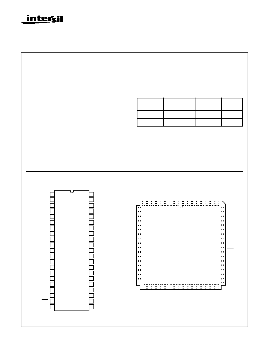
Pinouts
Ordering Information
PART
NUMBER
TEMP. RANGE
(
o
C)
PACKAGE
PKG. NO.
HI1396JCJ
-20 to 75
42 Ld SBDIP
D42.6
HI1396AIL
-20 to 100
68 Ld CLCC
J68.A
HI1396 (SBDIP)
TOP VIEW
HI1396 (CLCC)
TOP VIEW
13
1
2
3
4
5
6
7
8
9
10
11
12
14
15
16
17
18
19
20
AV
EE
NC
LINV
DV
EE
DGND1
DGND2
(LSB) D0
D1
D2
D3
D4
D5
D6
(MSB) D7
DGND2
DGND2
DV
EE
MINV
NC
CLK
30
42
41
40
39
38
37
36
35
34
33
32
31
29
28
27
26
25
24
NC
V
RT
NC
AV
EE
AV
EE
NC
NC
AGND
V
IN
AGND
V
RM
AGND
V
IN
AGND
NC
NC
AV
EE
AV
EE
NC
V
RB
21
22
23
NC
CLK
NC
NC
NC
NC
A
GND
V
IN
A
GND
V
RM
A
GND
V
IN
A
GND
NC
NC
NC
NC
NC
AV
EE
AV
EE
NC
V
RB
NC
NC
NC
CLK
CLK
NC
MINV
NC
DV
EE
NC
NC
NC
NC
AV
EE
AV
EE
NC
V
RT
NC
AV
EE
NC
NC
NC
LINV
NC
DV
EE
NC
DGND1
DGND2
NC
NC
NC
9
8
7
6
5
4
3
2
1 68 67 66 65 64 63 62 61
60
59
58
57
56
55
54
53
52
51
50
49
48
47
46
45
44
10
11
12
13
14
15
16
17
18
19
20
21
22
23
24
25
26
27 28 29 30 31 32 33 34 35 36 37 38 39 40 41 42 43
NC
NC
NC
NC
(LSB) D0
D1
D2
D3
D4
D5
D6
(MSB) D7
NC
DGND2
DGND1
NC
NC
File Number
3576.3
CAUTION: These devices are sensitive to electrostatic discharge; follow proper IC Handling Procedures.
http://www.intersil.com or 407-727-9207
|
Copyright
©
Intersil Corporation 1999
4-1157
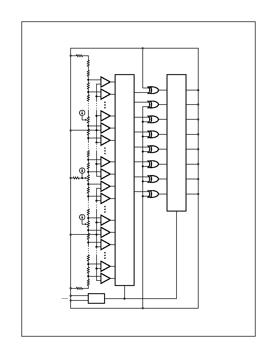
Functional Block Diagram
255
254
R/2
R
R
R3
193
R
191
R
192
R
128
R
127
R
126
R
R2
V
RM
V
IN
V
RB
CLOCK
DRIVER
65
R
63
R
64
R
2
R
1
V
IN
R
R/2
V
RT
R1
COMPARATOR
MINV
ENCODE
LOGIC
LINV
OUTPUT
D7 (MSB)
D6
D5
D4
D3
D2
D1
D0 (LSB)
CLK
CLK
129
R
HI1396
4-1158
Absolute Maximum Ratings
T
A
= 25
o
C
Thermal Information
Supply Voltage (AV
EE
, DV
EE
) . . . . . . . . . . . . . . . . . . . . . . . . . . .-7V
Analog Input Voltage (V
IN
) . . . . . . . . . . . . . . . . . . . . . -2.7V to +0.5V
Reference Input Voltage
V
RT
, V
RB
, V
RM
. . . . . . . . . . . . . . . . . . . . . . . . . . . -2.7V to +0.5V
|V
RT
- V
RB
| . . . . . . . . . . . . . . . . . . . . . . . . . . . . . . . . . . . . . . 2.5V
Digital Input Voltage
CLK, CLK, MINV, LINV . . . . . . . . . . . . . . . . . . . . . . . -4V to +0.5V
|CLK-CLK | . . . . . . . . . . . . . . . . . . . . . . . . . . . . . . . . . . . . . . . 2.7V
V
RM
Pin Input Current (I
VRM
) . . . . . . . . . . . . . . . . . . -3mA to +3mA
Digital Output Current (ID0 to ID7) . . . . . . . . . . . . . . . -30mA to 0mA
Thermal Resistance (Typical, Note 1)
JA
o
C/W
JC
o
C/W
SBDIP Package . . . . . . . . . . . . . . . . . .
45
7
CLCC Package . . . . . . . . . . . . . . . . . .
45
8
Maximum Junction Temperature
Ceramic Packages. . . . . . . . . . . . . . . . . . . . . . . . . . . . . . . 175
o
C
Maximum Storage Temperature Range (T
STG
) . . . .-65
o
C to 150
o
C
Maximum Lead Temperature (Soldering 10s) . . . . . . . . . . . . 300
o
C
Operating Conditions
(Note 1)
Temperature Ranges (Note 4)
SBDIP Package, T
A
. . . . . . . . . . . . . . . . . . . . . . . . -20
o
C to 75
o
C
CLCC Package, T
C
. . . . . . . . . . . . . . . . . . . . . . . . -20
o
C to 100
o
C
Supply Voltage Ranges
AV
EE
, DV
EE
. . . . . . . . . . . . . . . . . . . . . . . . . . . . . -5.5V to -4.95V
AV
EE
- DV
EE
. . . . . . . . . . . . . . . . . . . . . . . . . . . . . -0.05V to 0.05V
AGND - DGND . . . . . . . . . . . . . . . . . . . . . . . . . . . -0.05V to 0.05V
Reference Input Voltage
V
RT
. . . . . . . . . . . . . . . . . . . . . . . . . . . . . . . . . . . . . . -0.1V to 0.1V
V
RB
. . . . . . . . . . . . . . . . . . . . . . . . . . . . . . . . . . . . . -2.2V to -1.8V
Analog Input Voltage, V
IN
. . . . . . . . . . . . . . . . . . . . . . . . V
RB
to V
RT
Pulse Width of Clock
t
PW1
. . . . . . . . . . . . . . . . . . . . . . . . . . . . . . . . . . . . . . . 4.0ns (Min)
t
PW0
. . . . . . . . . . . . . . . . . . . . . . . . . . . . . . . . . . . . . . . 4.0ns (Min)
CAUTION: Stresses above those listed in "Absolute Maximum Ratings" may cause permanent damage to the device. This is a stress only rating and operation of
the device at these or any other conditions above those indicated in the operational sections of this specification is not implied.
NOTE:
1.
JA
is measured with the component mounted on an evaluation PC board in free air.
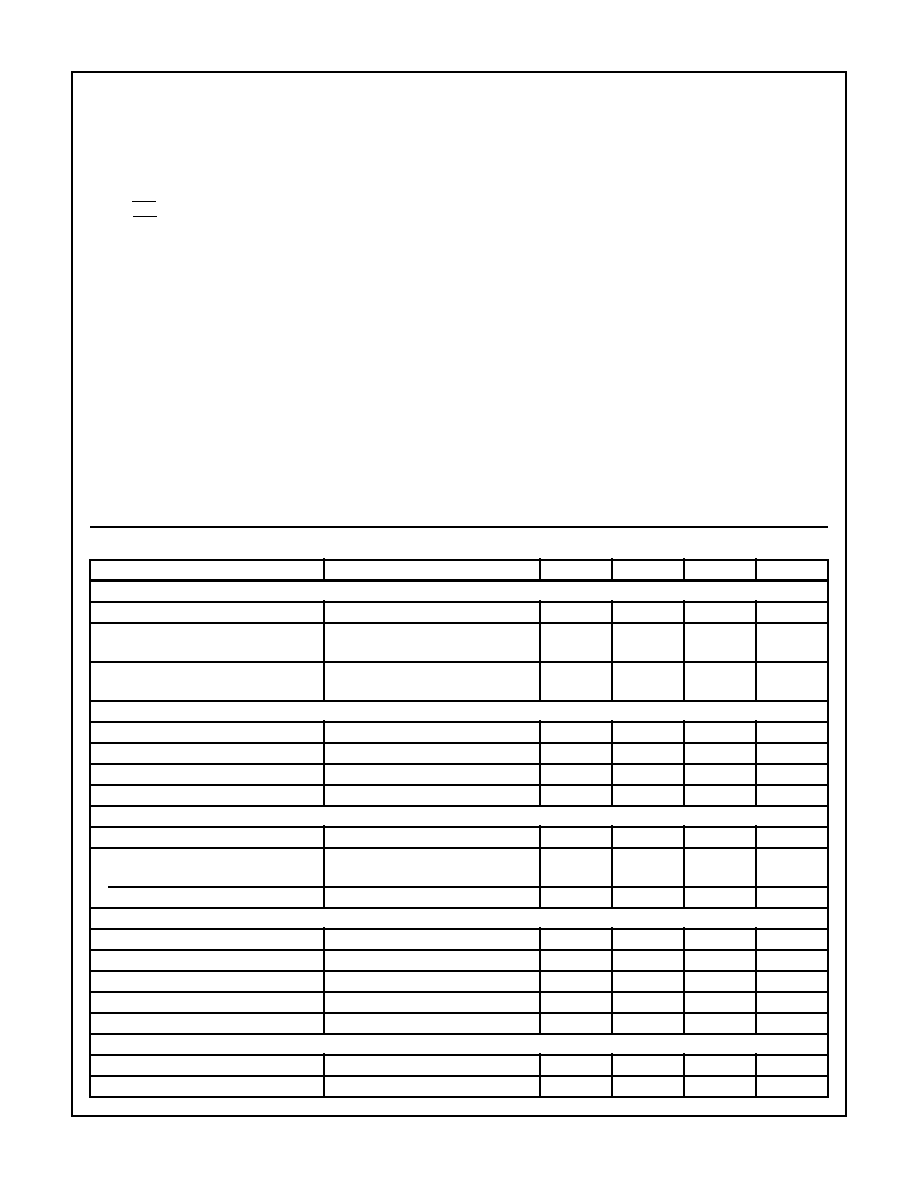
Electrical Specifications
T
A
= 25
o
C, AV
EE
= DV
EE
= -5.2V, V
RT
= 0V, V
RB
= -2V (Note 1)
PARAMETER
TEST CONDITIONS
MIN
TYP
MAX
UNIT
SYSTEM PERFORMANCE
Resolution
-
8
-
Bits
Integral Linearity Error, INL
HI1396JCJ, HI1396AIL
f
C
= 125 MSPS
-
±
0.3
±
0.5
LSB
Differential Linearity Error, DNL
HI1396JCJ, HI1396AIL
f
C
= 125 MSPS
-
-
±
0.5
LSB
ANALOG INPUT
Input Bandwidth
V
IN
= 2V
P-P
200
-
-
MHz
Analog Input Capacitance, C
IN
V
IN
= 1V + 0.07V
RMS
-
17
-
pF
Analog Input Resistance, R
IN
50
190
-
k
Input Bias Current, I
IN
V
IN
= -1V
20
130
400
µ
A
REFERENCE INPUTS
Reference Resistance, R
REF
75
110
155
Offset Voltage
E
OT
V
RT
8
19
32
mV
E
OB
V
RB
0
15
24
mV
DIGITAL INPUTS
Logic H Level, V
IH
-1.13
-
-
V
Logic L Level, V
IL
-
-
-1.50
V
Logic H Current, I
IH
Input Connected to -0.8V
0
-
50
µ
A
Logic L Current, I
IL
Input Connected to -1.6V
0
-
50
µ
A
Input Capacitance
-
7
-
pF
DIGITAL OUTPUTS
Logic H Level, V
OH
R
L
= 50
to -2V
-1.10
-
-
V
Logic L Level, V
OL
R
L
= 50
to -2V
-
-
-1.62
V
HI1396
4-1159
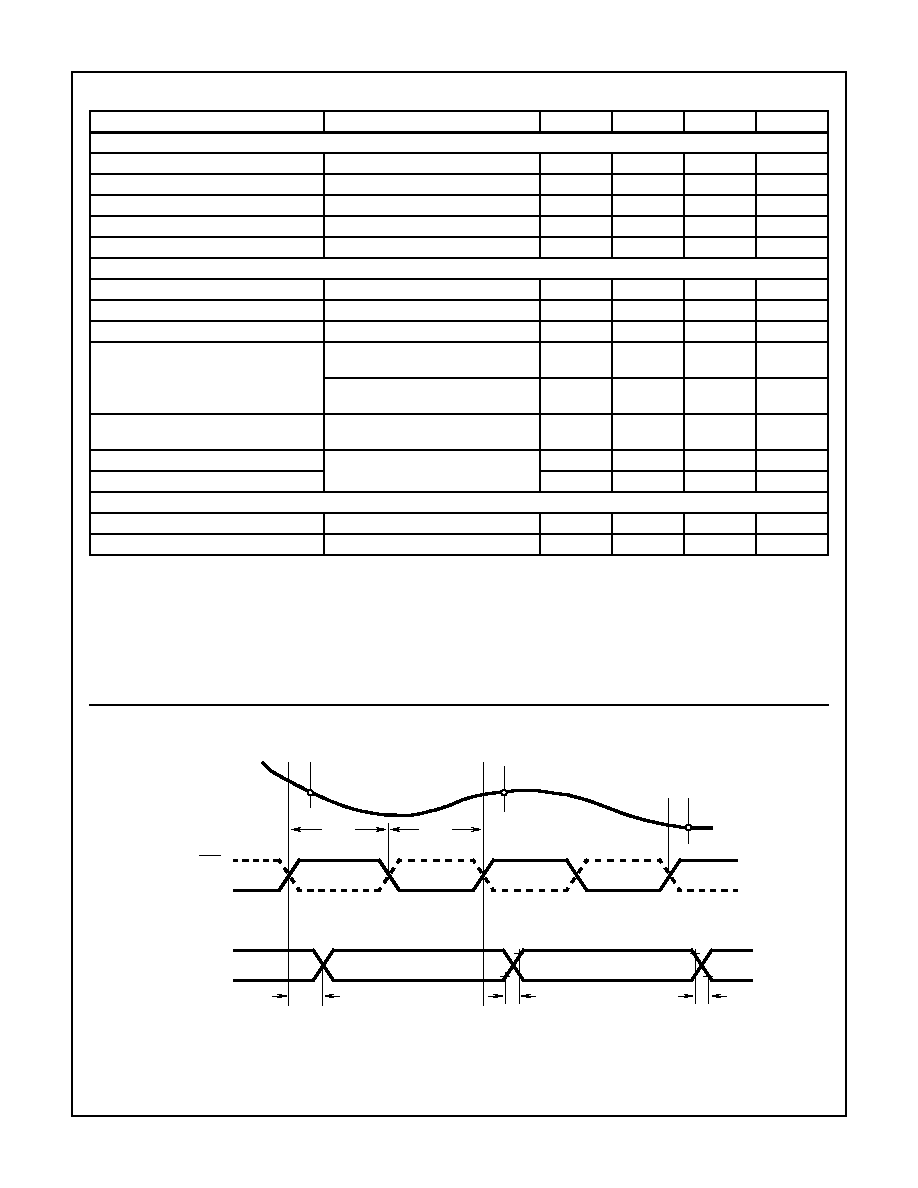
TIMING CHARACTERISTICS
Output Rise Time, t
r
R
L
= 50
to -2V, 20% to 80%
0.5
0.9
1.2
ns
Output Fall Time, t
f
R
L
= 50
to -2V, 20% to 80%
0.5
1.0
1.3
ns
Output Delay, t
OD
3.0
3.6
4.2
ns
H Pulse Width of Clock, t
PW1
4.0
-
-
ns
L Pulse Width of Clock, t
PW0
4.0
-
-
ns
DYNAMIC CHARACTERISTICS
Maximum Conversion Rate, f
C
Error Rate 10
-9
TPS (Note 2)
125
-
-
MSPS
Aperture Jitter, t
AJ
-
10
-
ps
Sampling Delay, t
DS
-
1.5
-
ns
Signal to Noise Ratio (SINAD)
Input = 1MHz, Full Scale
f
C
= 125 MSPS
-
46
-
dB
Input = 31.5MHz, Full Scale
f
C
= 125 MSPS
-
40
-
dB
Error Rate
Input = 31.249MHz, Full Scale
Error > 16 LSB, f
C
= 125 MSPS
-
-
10
-9
TPS
(Note 2)
Differential Gain Error, DG
NTSC 40 IRE Mod.
Ramp, f
C
= 125 MSPS
-
1.0
-
%
Differential Phase Error, DP
-
0.5
-
Degree
POWER SUPPLY CHARACTERISTICS
Supply Current, I
EE
-230
-160
-
mA
Power Consumption
Note 3
-
870
-
mW
NOTES:
1. Electrical Specifications guaranteed within stated operating conditions.
2. TPS: Times Per Sample.
3.
4. T
A
specified in still air and without heat sink. To extend temperature range, appropriate heat management techniques must be employed.
Electrical Specifications
T
A
= 25
o
C, AV
EE
= DV
EE
= -5.2V, V
RT
= 0V, V
RB
= -2V (Note 1) (Continued)
PARAMETER
TEST CONDITIONS
MIN
TYP
MAX
UNIT
RMS Signal
RMS Noise
Distor tion
+
------------------------------------------------------------------
=
P
D
I
EE
V
EE
∑
V
RT
V
RB
≠
(
)
2
R
REF
-------------------------------------
+
=
Timing Diagram
FIGURE 1.
N
N + 1
N + 2
N + 1
N
N - 1
20%
80%
t
r
t
OD
t
f
t
PW1
t
PW0
20%
80%
ANALOG IN
CLK
CLK
DIGITAL OUT
HI1396

4-1160
Pin Descriptions and I/O Pin Equivalent Circuits
PIN NUMBER
SYMBOL
I/O
STANDARD
VOLTAGE
LEVEL
EQUIVALENT CIRCUIT
DESCRIPTION
DIP
LCC
29, 31,
33, 35
49, 51,
53, 55
AGND
-
0V
Analog GND. Used as GND for
input buffers and latches of
comparators. Isolated from
DGND1, DGND2.
1, 25,
26, 38,
39
41, 42,
62, 63,
67
AV
EE
-
-5.2V
Analog V
EE
-5.2V (Typ). Internally
connected to DV
EE
(Resistance:
4
to 6
). Bypass with 0.1
µ
F to
AGND.
21
35
CLK
I
ECL
CLK Input.
20
34
CLK
Input complementary to CLK.
When left open pulled down to
-1.3V. Device is operable without
CLK input, but use of
complementary inputs of CLK and
CLK is recommended to obtain
stable high speed operation.
5, 16
7, 24
DGND1
-
0V
Digital GND for internal circuits.
6, 15
8, 23
DGND2
-
0V
Digital GND for output transistors.
4, 17
5, 30
DV
EE
-
-5.2V
Digital V
EE
. Internally connected
to AV
EE
(resistance: 4
to 6
).
Bypass with 0.1
µ
F to DGND
7
14
D0
O
ECL
LSB of data outputs. External
pull-down resistor is required.
8
15
D1
Data outputs. External pull-down
resistors are required.
9
16
D2
10
17
D3
11
18
D4
12
19
D5
13
20
D6
14
21
D7
MSB of data outputs. External
pull-down resistor is required.
DV
EE
CLK
CLK
DGND1
R
R
R
R
R
R
DV
EE
DGND2
DI
HI1396