1
®
December 1997
HI-7151
10-Bit, High Speed, A/D Converter
with Track and Hold
Features
· Conversion Time . . . . . . . . . . . . . . . . . . . . . . . . . . . 10
µs
· Continuous Throughput Rate . . . . . . . . . . . . . . . 100kHz
· No Offset or Gain Adjustments Necessary
· Internal Track and Hold Amplifier
· Analog and Reference Inputs Fully Buffered
·
µP Compatible Byte Organized Outputs
· Low Power Consumption . . . . . . . . . . . . . . . . . . 150mW
· Uses a Single 2.5V Reference for
±2.5 V Input Range
Applications
·
µP Controlled Data Acquisition Systems
· DSP
- Avionics
- Sonar
· Process Control
- Automotive Transducer Sensing
- Industrial
· Robotics
· Digital Communications
· Image Processing
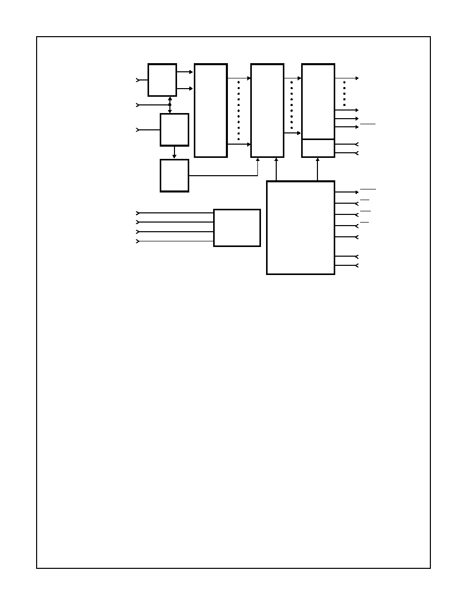
Description
The Intersil HI-7151 is a high speed 10-bit A/D converter
which uses a 2-Step Flash algorithm to achieve throughput
rates of 100kHz. A unique switched capacitor technique
allows a new input voltage to be sampled while a conversion
is taking place.
A Track and Hold amplifier is included on the chip, consisting
of two high speed amplifiers and an internal hold capacitor.
Microprocessor bus interfacing is simplified by the use of
standard Chip Select, Read, and Write control signals. The
digital three-state outputs are byte organized for interfacing
the either 8- or 16-bit systems. An Over-Range pin, together
with the MSB, can be used to indicate an out-of-range
condition.
The HI-7151 operates with
±5V supplies. A single +2.5V
reference is required to provide a bipolar input range from
-2.5V to +2.5V.
Internal high speed CMOS buffers at both the analog and
reference inputs simplify external drive requirements.
Pinout
HI-7151
(PDIP, CERDIP)
TOP VIEW
Ordering Information
PART
NUMBER
LINEARITY
(MAX. DLE)
TEMP.
RANGE (
o
C)
PACKAGE
HI3-7151J-5
±1 LSB
0 to 75
28 Ld PDIP
HI3-7151K-5
±
1
/
2
LSB
0 to 75
28 Ld PDIP
HI3-7151A-9
±1 LSB
0 to 85
28 Ld PDIP
HI3-7151B-9
±
1
/
2
LSB
0 to 85
28 Ld PDIP
HI1-7151S-2
±1 LSB
-55 to 125
28 Ld CERDIP
HI1-7151T-2
±
1
/
2
LSB
-55 to 125
28 Ld CERDIP
GND
V-
V
REF
AG
V
IN
SET
BUSY
CLK
HOLD
WR
CS
RD
SMODE
DG
V+
D9
D8
D7
D6
D4
D2
D1
D0
HBE
BUS
OVR
D5
D3
28
27
26
25
24
23
22
21
20
19
18
17
16
15
1
2
3
4
5
6
7
8
9
10
11
12
13
14
CAUTION: These devices are sensitive to electrostatic discharge; follow proper IC Handling Procedures.
1-888-INTERSIL or 321-724-7143
|
Intersil (and design) is a registered trademark of Intersil Americas Inc.
Copyright © Intersil Americas Inc. 2002. All Rights Reserved
File Number
3099.1
NOT
REC
OMM
END
ED F
OR N
EW D
ESIG
NS
3
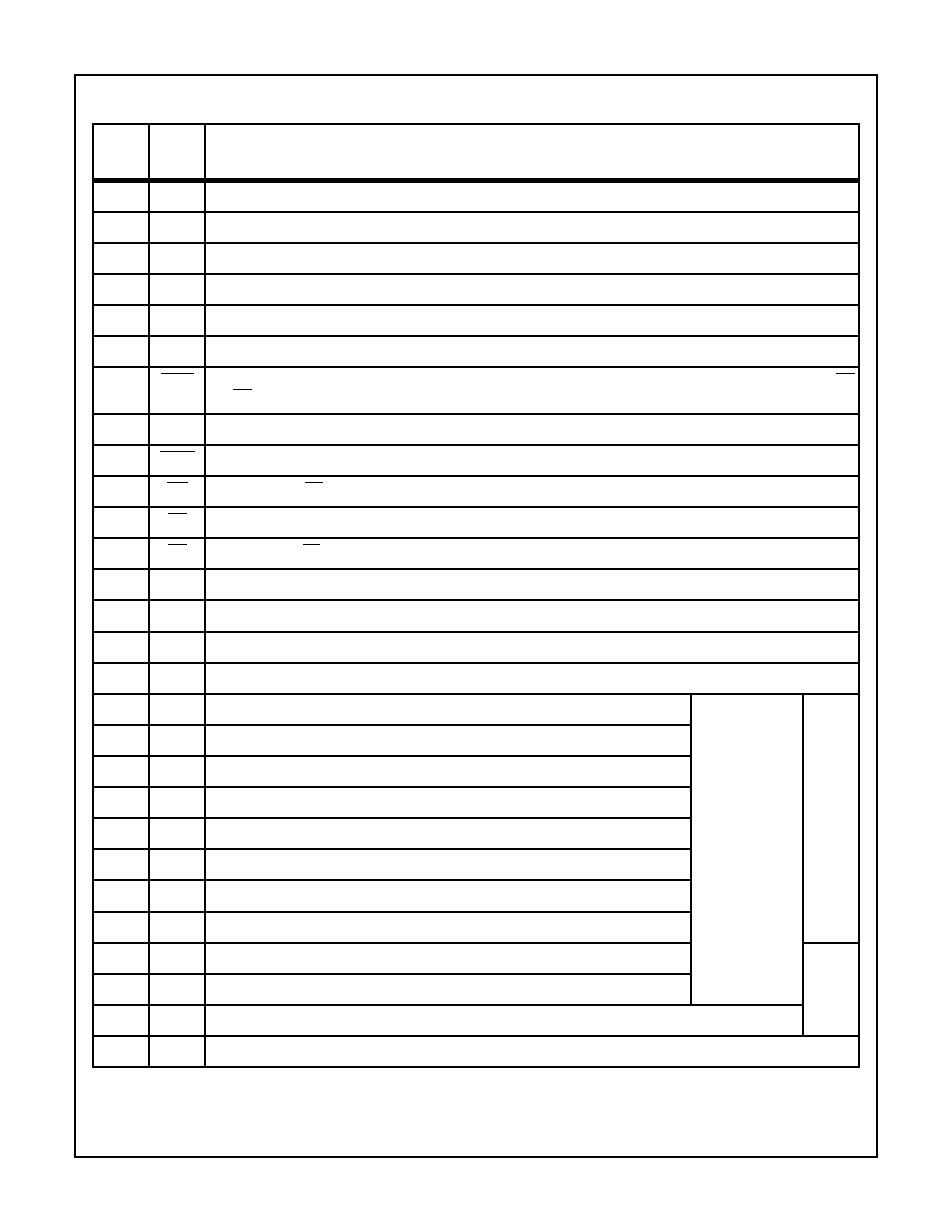
Pin Descriptions
PIN
NAME
DESCRIPTION
1
GND
Ground return for comparators (0V).
2
V-
Negative supply voltage input (-5V).
3
V
REF
Reference voltage input (+2.5V).
4
AG
Analog ground reference (0V).
5
V
IN
Analog Input Voltage.
6
SET
Connect to V+ for proper operation.
7
BUSY
Output High-Conversion complete. Output Low - Conversion in progress. Output floats when chip is not selected (RD
and CS both high).
8
CLK
Clock input.
9
HOLD
Indicates start of conversion. Active low.
10
WR
Write input. With CS low, starts conversion when pulsed low; continuous conversions when kept low.
11
CS
Chip select input. Active low.
12
RD
Read input. With CS low, enables output buffers when pulsed low; outputs updated at end of conversion when kept low.
13
SMODE Slow memory mode input. Active high.
14
DG
Digital ground (0V).
15
BUS
Bus select input. High = all outputs enabled together D0 - D9, OVR. Low = outputs enabled by HBE.
16
HBE
Byte select (HBE/LBE) input for 8-bit bus. Input high-High byte select, D8-D9, OVR Input low-low byte select, D0-D7.
17
D0
Bit 0 (Least significant, LSB).
Output Data Bits
(High = True)
Low
Byte
18
D1
Bit 1.
19
D2
Bit 2.
20
D3`
Bit 3.
21
D4
Bit 4.
22
D5
Bit 5.
23
D6
Bit 6.
24
D7
Bit 7.
25
D8
Bit 8 (Most Significant).
High
Byte
26
D9
Bit 9 (Sign).
27
OVR
Out of Range flag. Valid at end of conversion when output exceeds full scale.
28
V+
Positive supply voltage input (+5V).
HI-7151

4
Absolute Maximum Ratings
(Note 1)
Thermal Information
Supply Voltage
V+ to Gnd (DG/AG/GND) . . . . . . . . . . . . . . . . -0.3V < V+ < +5.7V
V- to Gnd (DG/AG/GND). . . . . . . . . . . . . . . . . .-5.7V < V- < +0.3V
Analog Input Pins . . . . . . . . . . . . . . . . . V- -0.3V < V
INA
< V+ +0.3V
Digital I/O Pins . . . . . . . . . . . . . . . . . . .DG - 0.3V < V
I/O
< V+ +0.3V
Operating Conditions
Temperature Range
HI3-7151X-5 . . . . . . . . . . . . . . . . . . . . . . . . . . . . . . . .0
o
C to 75
o
C
HI3-7151X-9 . . . . . . . . . . . . . . . . . . . . . . . . . . . . . . -40
o
C to 85
o
C
Thermal Resistance (Typical)
JA
(
o
C/W)
JC
(
o
C/W)
PDIP Package . . . . . . . . . . . . . . . . . . .
__
N/A
CERDIP Package . . . . . . . . . . . . . . . .
__
__
Maximum Power Dissipation (Note 2). . . . . . . . . . . . . . . . . <500mW
Maximum Storage Temperature Range . . . . . . . . . . -65
o
C to 150
o
C
Maximum Lead Temperature (Soldering, 10s) . . . . . . . . . . . . 300
o
C
CAUTION: Stresses above those listed in "Absolute Maximum Ratings" may cause permanent damage to the device. This is a stress only rating and operation
of the device at these or any other conditions above those indicated in the operational sections of this specification is not implied.
NOTES:
1. Input voltages may exceed the supply voltage provided the inputs current is limited to
±1mA.
2. Dissipation rating assumes device is mounted with all leads soldered to printed circuit board (derate above 75
o
C at -10mW/
o
C).
Electrical Specifications
V+ = +5V, V- = -5V, V
REF
= 2.5V, f
CLK
= 300kHz, 50% Duty Cycle, Unless Otherwise Specified (Note 4)
PARAMETER
SYMBOL
(NOTE 3)
TEMPERATURE
J, A GRADE
K, B GRADE
UNITS
MIN
TYP
MAX
MIN
TYP
MAX
ACCURACY
Resolution (Note 5) (With
no missing codes)
RES
T
A
= -25
o
C
10
-
-
10
-
-
Bits
T
MIN
to T
MAX
10
-
-
10
-
-
Bits
Integral Linearity Error
ILE
T
A
= 25
o
C
-
±0.5
±1.0
-
±0.3
±-0.5
LSB
T
MIN
to T
MAX
-
±0.75
±1.0
-
±0.5
±0.75
LSB
Differential Linearity Error
DLE
T
A
= 25
o
C
-
-
±1.0
-
-
±0.5
LSB
T
MIN
to T
MAX
-
-
±1.0
-
-
±0.75
LSB
Bipolar Offset Error
V
OS
T
A
= 25
o
C
-
±1.0
±2.5
-
±0.6
±1.5
LSB
T
MIN
to T
MAX
-
±1.5
±3.0
-
±1.0
±2.0
LSB
Unadjusted Gain Error
eG+ and
eG-
T
A
= 25
o
C
-
±1.0
±2.5
-
±0.6
±1.5
LSB
T
MIN
to T
MAX
-
±1.5
±3.0
-
±1.0
±2.0
LSB
NOTE:
3. T
MIN
to T
MAX
: See Ordering Information Table.
DC Electrical Specifications
V+ = 5V, V- = -5V, V
REF
= 2.5V, T
A
= 25
o
C, f
CLK
= 300kHz, 50% Duty Cycle,
Unless Otherwise Specified
PARAMETER
SYMBOL
(NOTE 4)
CONDITIONS
25
o
C
0
o
C to 75
o
C
-40
o
C to 85
o
C
UNITS
MIN
TYP
MAX
MIN
MAX
MIN
MAX
ANALOG INPUT
Analog Input Range
V
IR
V
IN
= 0V
-V
REF
-
V
REF
-V
REF
V
REF
-V
REF
V
REF
V
Analog INput Bias Current
I
BI
-
0.01
100
-
100
-
100
nA
Analog Input Capacitance
(Note 5)
CV
IN
-
8
20
-
-
-
-
pF
REFERENCE INPUT
Reference Input Range
(Note 6)
V
RR
V
REF
= 2.5V
2.2
2.5
2.6
2.2
2.6
2.2
2.6
V
Reference Input Bias Current
I
BR
-
0.01
100
-
100
-
100
nA
Reference Input Capacitance
(Note 5)
CV
R
-
7
20
-
-
-
-
pF
HI-7151

5
TRACK AND HOLD (See Text)
Slew Rate
SR
-
9
-
-
-
-
-
V/
µs
Bandwidth
BW
-
1.5
-
-
-
-
-
MHz
Aperture Time
-
30
-
-
-
-
-
ns
Aperture Uncertainty
-
2
-
-
-
-
-
ns
Feedthrough in HOLD
f
IN
= 100kHz
-
-80
-
-
-
-
-
dB
Acquisition Time
-
1.5
-
-
-
-
-
µs
LOGIC INPUTS
Input High Voltage
V
IH
2.0
-
-
2.0
-
2.0
-
V
Input Low Voltage
V
IL
-
-
0.8
-
0.8
-
0.8
V
Logic Input Current
I
IL
V
IN
= 0V, V+
-
0.05
1
-
1
-
1
µA
Input Capacitance (Note 5)
C
IN
-
5
17
-
-
-
-
pF
LOGIC OUTPUTS
Output High Voltage
V
OH
I
OH
= -200
µA
2.4
-
-
2.4
-
2.4
-
V
Output Low Voltage
V
OL
I
OL
= 1.6mA
-
-
0.4
-
0.4
-
0.4
V
Output Leakage Current
I
OL
RD = V+, V
OUT
= V+
-
0.04
1
-
10
-
10
µA
RD = V+, V
OUT
= 0V
-1
-0.01
-
-10
-
-10
-
µA
Output Capacitance (Note 5)
C
OUT
High-Z State
-
7
15
-
-
-
-
pF
POWER SUPPLY VOLTAGE RANGE
(Note 7)
V+
Function Operation
Only
4.5
5.0
5.5
4.5
5.5
4.5
5.5
V
(Note 7)
V-
-4.5
-5.0
-5.5
-4.5
-5.5
-4.5
-5.5
V
POWER SUPPLY REJECTION
V+, V- Gain Coefficient
eGVS
V+ = 5V, V- = -4.75V,
-5.25V
-
±0.1
±0.05
-
±0.6
-
±0.6
LSB
V- = -5V, V+ = 4.75V,
5.25V
-
±0.1
±0.5
-
±0.6
-
±0.6
LSB
V+, V- Offset Coefficient
VOSVS
V+ = 5V, V- = -4.75V,
-5.25V
-
±0.1
±0.5
-
±0.6
-
±0.6
LSB
V- = -5V, V+ = 4.75V,
5.25V
-
±0.1
±0.5
-
±0.6
-
±0.6
LSB
SUPPLY CURRENTS
V+ Supply Current
I+
V+ = 5V
±10%
V- = -5V
±10%
V
IN
= 0V, Digital
Outputs are
Unloaded
-
20
30
-
30
-
30
mA
V- Supply Current
I-
-
-10
-15
-
-15
-
-15
mA
GND Current
I
GND
-
-8
-15
-
-15
-
-15
mA
DG Current
I
DG
-
-2
-3
-
-3
-
-3
mA
AG Current
I
AG
-
0.02
10
-
10
-
10
µA
NOTES:
4. FSR (Full Scale Range) = 2 X V
REF
(5V at V
REF
= 2.5V). LSB (Least Significant Bit) = FSR/1024 (4.88mV at V
REF
= 2.5V)
5. Parameter not tested. Parameter guaranteed by design, simulation, or characterization.
6. Only V
OS
and GAIN ERROR functionality tested at 2.2V and 2.6V.
7. Guaranteed by functionality test.
DC Electrical Specifications
V+ = 5V, V- = -5V, V
REF
= 2.5V, T
A
= 25
o
C, f
CLK
= 300kHz, 50% Duty Cycle,
Unless Otherwise Specified (Continued)
PARAMETER
SYMBOL
(NOTE 4)
CONDITIONS
25
o
C
0
o
C to 75
o
C
-40
o
C to 85
o
C
UNITS
MIN
TYP
MAX
MIN
MAX
MIN
MAX
HI-7151