 | –≠–ª–µ–∫—Ç—Ä–æ–Ω–Ω—ã–π –∫–æ–º–ø–æ–Ω–µ–Ω—Ç: HI1866 | –°–∫–∞—á–∞—Ç—å:  PDF PDF  ZIP ZIP |

4-1
Semiconductor
[ /Title (HI1866)
/Subject (6-Bit, 140 MSPS, Flash A/D Converter)
/Author ()
/Keywords (Harris Semiconductor, RGB, Video, Flat
Panel, LCD)
/Creator ()
/DOCINFO pdfmark
[ /PageMode /UseOutlines
/DOCVIEW pdfmark
October 1998
HI1866
6-Bit, 140 MSPS, Flash A/D Converter
Features
∑ Ultra-High Speed Operation with Maximum
Conversion Rate. . . . . . . . . . . . . . . . . . . . . . . 140 MSPS
∑ Low Input Capacitance . . . . . . . . . . . . . . . . . . . . . . . 7pF
∑ Wide Analog Input Bandwidth . . . . . . . . . . . . . 210MHz
∑ Low Power Consumption . . . . . . . . . . . . . . . . . .325mW
∑ Low Error Rate
∑ Excellent Temperature Characteristics
∑ 1:2 Demultiplexed Output (TTL Level)
∑ Direct Replacement for Sony CXA1866
Applications
∑ LCD Panels
∑ Magnetic Recording (PRML)
∑ Communications (QPSK, QAM)
Description
HI1866 is a 6-bit, high-speed, flash A/D converter capable of
digitizing analog signals at the maximum rate of 140 MSPS.
The digital input level is compatible with the ECL
100K/10KH/10K.
Pinout
HI1866
(MQFP)
TOP VIEW
Ordering Information
PART
NUMBER
TEMP.
RANGE (
o
C)
PACKAGE
PKG. NO.
HI1866JCQ
-20 to 75
48 Ld MQFP
Q48.12x12-S
1
2
3
4
5
6
7
8
32
31
30
29
28
27
26
25
24
23
22
21
20
19
18
17
9
10
11
12
13 14 15 16
33
34
35
36
37
38
39
40
41
42
43
44
45
46
47
48
DGND3
P1D5 (MSB)
P1D4
P1D3
P1D2
P1D1
P1D0 (LSB)
DGND3
DV
CC2
INV
CCLK
NCCLK
DGND3
P2D0 (LSB)
P2D1
P2D2
P2D3
DGND3
DV
CC2
NC
DCLK
NDCLK
P2D4
P2D5 (MSB)
DV
CC2
DV
CC1
DGND1
DGND2
DV
EE
DGND3
DV
EE
DGND2
DGND1
DV
CC1
DV
CC2
DV
CC2
NC
AV
EE
V
RBS
V
RB
A
GND
NC
V
IN
A
GND
V
RT
V
RT
S
AV
EE
NC
CAUTION: These devices are sensitive to electrostatic discharge. Users should follow proper IC Handling Procedures.
Copyright
©
Harris Corporation 1997
File Number
4108.2
NOT RECOMMENDED FOR NEW DESIGNS
See HI3086
4-2
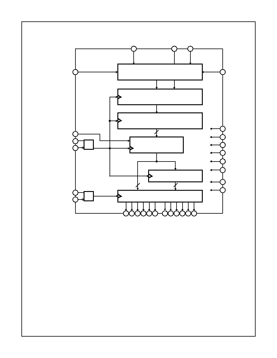
Functional Block Diagram
7
6
5
4
3
2
35 34 33 32 31 30
P2D5 (MSB)
P2D4
P2D3
P2D2
P2D1
P2D0 (LSB)
PD15 MSB)
P1D4
P1D3
P1D2
P1D1
P1D0 (LSB)
CLATCH B
TTLOUT
48
47
42
45
46
20
23
41
6
6
CLATCH A
CD
12
11
CD
25
26
27
6
6-BIT LATCH
COMPARATOR
16
21 V
RT
D
VEE
A
VEE
AGND
DGND1
DGND2
DGND3
DV
CC1
DV
CC2
REFERENCE RESISTANCE CHAIN
19
22
15
V
RBS
V
IN
V
RTS
V
RTS
INV
CCLK
NCCLK
DCLK
NDCLK
CD: CLOCK DRIVER
HI1866

4-3
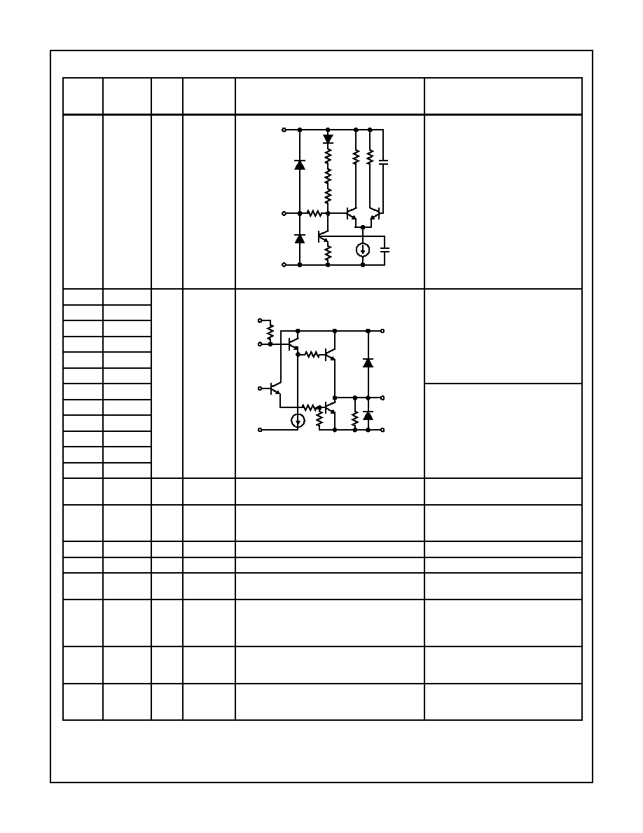
Pin Descriptions
PIN NO.
SYMBOL
I/O
TYPICAL
VOLTAGE
LEVEL
EQUIVALENT CIRCUIT
DESCRIPTION
21
V
RT
I
0V
Top reference voltage input (= 0). This is
the top reference voltage supplied to the
internal resistance chain. The external
input can be set in accordance with the
peak value on the plus side of the input
analog signal amplitude.
22
V
RTS
O
0V
V
RT
sense output. This is the voltage
sense pin for V
RT
.
16
V
RB
I
-2V
Bottom reference voltage input (= -2V).
This is the bottom reference voltage
supplied to the internal resistance
chain. The external input can be set in
accordance with the peak value on the
minus side of the input analog signal
amplitude.
15
V
RBS
O
-2V
V
RB
sense output. This is the voltage
sense pin for V
RB
.
19
V
IN
I
V
RTS
to
V
RBS
Analog input. The input range is 2V
P-P
.
26
CCLK
I
ECL
CCLK clock input. This is the conversion
clock, and is an ECL level input.
25
NCCLK
I
ECL
CCLK inversion clock input. This is an
ECL level input. When left open, this
input goes to the ECL threshold potential
(-1.3V). Only CCLK input can be used for
operation with the NCCLK input left
open, but complementary input is
recommended to attain fast and stable
operation.
11
DCLK
I
ECL
DCLK clock input. This is the 1:2 DMPX
latch clock; input a clock of
1
/
2
frequency
of CCLK. Data is output from DMPX port
1 and port 2 synchronously with the
rising edge of this signal. This is an ECL
level input.
12
NDCLK
I
ECL
DCLK inversion clock input. This is an
ECL level input. When left open, this
input goes to the ECL threshold potential
(-1.3V). Only DCLK input can be used for
operation with the NDCLK input left
open, but complementary input is
recommended to attain fast and stable
operation.
V
RT
V
RTS
V
RBS
V
RB
COMPARATOR 1
COMPARATOR 2
COMPARATOR 31
COMPARATOR 32
COMPARATOR 63
V
IN
AGND
A
VEE
DGND1
CCLK
(DCLK)
NCCLK
(NDCLK)
500
500
D
VEE
1.3V
R
R
R
R
R
R
HI1866
4-4
27
INV
I
ECL
Digital output polarity inversion input.
This is an ECL level input. This input
inverts the polarity of the digital outputs
P1D0 to P1D5, and P2D0 to P2D5.
(Refer to the Output Code Table.) When
left open, this signal is maintained at the
low level.
30
P1D0
O
TTL
These pins are for the 6 bits of digital
output data for DMPX port 1. P2D5 is the
MSB, and P2D0 is the LSB. These are
TTL levels outputs.
31
P1D1
32
P1D2
33
P1D3
34
P1D4
35
P1D5
2
P2D0
These pins are for the 6 bits of digital
output data for DMPX port 2. P2D5 is the
MSB, and P2D0 is the LSB. These are
TTL level outputs.
3
P2D1
4
P2D2
5
P2D3
6
P2D4
7
P2D5
38, 47
DVCC1
-
+5.0V
+5V power supply for TTL level internal
circuit.
9, 28,
37, 43,
48
DVCC2
-
+5.0V
+5V power supply for TTL level output
buffers (P1D0 to P2D5).
39, 46
DGND1
-
0V
Ground for DV
EE
digital circuit.
40, 45
DGND2
-
0V
Ground for DV
CC1
digital circuit.
1, 8, 29,
36, 42
DGND3
-
0V
Ground for DV
CC2
digital circuit.
17, 20
AGND
-
0V
Ground for AV
EE
analog circuit. Used as
the ground for the comparator input
buffers, latches, etc. Separated from
DGND.
41, 44
DV
EE
-
-5.2V
-5.2V power supply for digital circuit.
Connected internally with AV
EE
.
(Resistance is 4
to 6
.)
14, 23
AV
EE
-
-5.2V
-5.2V power supply for analog circuit.
Connected internally with DV
EE
.
(Resistance is 4
to 6
.)
Pin Descriptions
(Continued)
PIN NO.
SYMBOL
I/O
TYPICAL
VOLTAGE
LEVEL
EQUIVALENT CIRCUIT
DESCRIPTION
INV
DGND1
D
VEE
1.3V
1.3V
500
R
R
R
R
DV
CC1
DV
CC2
P1D0 TO D5
P2D0 TO D5
DGND3
DGND2
100K
HI1866
4-5
Absolute Maximum Ratings
Thermal Information
Supply Voltage (AV
EE
, DV
EE
) . . . . . . . . . . . . . . . . . . . . -7V to 0.5V
(DV
CC
) (Note 2). . . . . . . . . . . . . . . . . . . .0.5V to 7.0V
Reference Voltage (V
RT
, V
RB
) . . . . . . . . . . . . . . . . . . . -2.7V to 0.5V
(
V
RT
- V
RB
). . . . . . . . . . . . . . . . . . . . . . . . . 2.5V
Analog Input Voltage (V
IN
) . . . . . . . . . . . . . . . . . . . . . . -2.7V to 0.5V
Digital Input Voltage (DIN) (Note 3) . . . . . . . . . . . . . . . -4.0V to 0.5V
(
CCLK≠NCCLK
,
DCLK≠NDCLK
) . . . . 2.5V
Digital Output Current (I
D0
to I
D6
) . . . . . . . . . . . . . -30mA to +30mA
Storage Temperature (T
STG
) . . . . . . . . . . . . . . . . . . -65
o
C to 150
o
C
Ambient Operating Temperature (T
A
) . . . . . . . . . . . . . -20
o
C to 75
o
C
Allowable Power Dissipation (P
D
). . . . . . . . . . . . . . . . . . . . . 750mW
Thermal Resistance (Typical, Note 1)
JA
(
o
C/W)
MQFP Package . . . . . . . . . . . . . . . . . . . . . . . . . . . .
95
Maximum Junction Temperature . . . . . . . . . . . . . . . . . . . . . . . 150
o
C
Maximum Storage Temperature Range (T
STG
) . . . -65
o
C to 150
o
C
Maximum Lead Temperature (Soldering 10s) . . . . . . . . . . . . . 300
o
C
(Lead Tips Only)
Recommended Operating Conditions
Supply Voltage
MIN
TYP
MAX
AV
EE
, DV
EE
. . . . . . . . . . . . . . . . . . . . . . . -5.5V
-5.2V
-4.75V
AV
EE
- DV
EE
. . . . . . . . . . . . . . . . . . . . . . .-0.05V
0V
0.05V
AGND - DGND (Note 4) . . . . . . . . . . . . . - 0.05V
0V
0.05V
DV
CC
(Note 5). . . . . . . . . . . . . . . . . . . . . . 4.75V
5.0V
5.25V
Temperature Range (T
A
) . . . . . . . . . . . . . . . -20
o
C
-
75
o
C
Reference Input Voltage
MIN
TYP
MAX
V
RT
. . . . . . . . . . . . . . . . . . . . . . . . . . . . . -0.1V
0V
0.1V
V
RB
. . . . . . . . . . . . . . . . . . . . . . . . . . . . . -2.2V
-2.0V
-0.8V
Analog Input Voltage (V
IN
) . . . . . . . . . . . . .
V
RB
To
V
RT
Digital Input Voltage, DIN (H) . . . . . . . . . . . -1.1V
-
-
DIN (L)
-
-
-1.5V
CCLK, NCCLK Frequency (f
CCLK
)(MHz) . .
-
-
140
DCLK, NDCLK Frequency (f
DCLK
)(MHz) . .
-
-
70
CCLK, NCCLK Duty (D
CCLK
)(%) . . . . . . . .
40
50
60
DCLK, NDCLK Duty (D
DCLK
)(%) . . . . . . . .
40
50
60
CCLK-DCLK Time Difference (t
DCD
)(ns). . . . -t
PWL
+ 2 0
t
PWH
+ 1
CAUTION: Stresses above those listed in "Absolute Maximum Ratings" may cause permanent damage to the device. This is a stress only rating and operation
of the device at these or any other conditions above those indicated in the operational sections of this specification is not implied.
NOTES:
1.
JA
is measured with the component mounted on an evaluation PC board in free air.
2. DV
CC
= DV
CC1
, DV
CC2
.
3. D
IN
= CCLK, NCCLK, DCLK, NDCLK, INV.
4. DGND = DGND1, DGND2, DGND3.
5. Refer to Timing Chart 1 for t
PWL
, t
PWH
.
Electrical Specifications
T
A
= 25
o
C, AV
EE
= DV
EE
= -5.2V, DV
CC
= 5V, V
RT
= 0V, V
RB
= -2V
PARAMETER
SYMBOL
TEST CONDITIONS
MIN
TYP
MAX
UNITS
Resolution, n
n
-
6
-
bits
DC CHARACTERISTICS
Integral Linearity Error
E
IL
f
C
= 140MHz
-
-
±
0.2
LSB
Differential Linearity Error
E
DL
f
C
= 140MHz
-
-
±
0.2
LSB
No Missing Code
-
Guar-
anteed
-
-
ANALOG INPUT
Analog Input Capacitance
C
IN
V
IN
= -1V_0.7V
RMS
, DC
-
7
-
pF
Analog Input Resistance
R
IN
-2V
V
IN
0V
200
-
-
K
Input Bias Current
I
IN
-2V
V
IN
0V
-
-
110
µ
REFERENCE INPUT
Reference Resistance
R
REF
-
225
-
Reference Resistance Current
I
REF
-
9
-
mA
Offset Voltage
V
RT
E
OT
0
-
25
mV
V
RB
E
OB
-
-
25
mV
DIGITAL INPUT
Logic High Level
V
IH
-1.13
-
-
V
HI1866