10-1197
August 1997
Features
∑ Throughput Rate . . . . . . . . . . . . . . . . . . . . . . . . 160MHz
∑ Resolution (HI20201) . . . . . . . . . . . . . . . . . . . . . . . 10-Bit
∑ Differential Linearity Error . . . . . . . . . . . . . . . . 0.5 LSB
∑ Low Glitch Noise
∑ Analog Multiplying Function
∑ Low Power Consumption . . . . . . . . . . . . . . . . . .420mW
∑ Evaluation Board Available
∑ Direct Replacement for Sony CX20201-1, CX20202-1
Applications
∑ Wireless Communications
∑ Signal Reconstruction
∑ Direct Digital Synthesis
∑ High Definition Video Systems
∑ Digital Measurement Systems
∑ Radar
Description
The HI20201 is a 160MHz ultra high speed D/A converter. The
converter is based on an R/2R switched current source archi-
tecture that includes an input data register with a complement
feature and is Emitter Coupled Logic (ECL) compatible.
The HI20201 is available in a commercial temperature range
and offered in a 28 lead plastic SOIC (300 mil) and a 28 lead
plastic DIP package.
Pinout
HI20201
(PDIP, SOIC)
TOP VIEW
Ordering Information
PART
NUMBER
TEMP.
RANGE (
o
C)
PACKAGE
PKG. NO.
HI20201JCB
-20 to 75
28 Ld SOIC
M28.3A-S
HI20201JCP
-20 to 75
28 Ld PDIP
E28.6A-S
HI20201-EV
25
Evaluation Kit
(MSB) D9
D8
D7
D6
D5
D4
D3
D2
D1
(LSB) D0
NC
NC
CLK
CLK
AV
SS
AV
EE
NC
NC
NC
NC
NC
AV
SS
DV
SS
COMPL
DV
EE
V
REF
NC
I
OUT
28
27
26
25
24
23
22
21
20
19
18
17
16
15
1
2
3
4
5
6
7
8
9
10
11
12
13
14
File Number
3581.5
HI20201
10-Bit, 160 MSPS,
Ultra High Speed D/A Converter
CAUTION: These devices are sensitive to electrostatic discharge; follow proper IC Handling Procedures.
http://www.intersil.com or 407-727-9207
|
Copyright
©
Intersil Corporation 1999
10-1199
Absolute Maximum Ratings
Thermal Information
Digital Supply Voltage DV
EE
to DV
SS
. . . . . . . . . . . . . . . . . . . -7.0V
Analog Supply Voltage AV
DD
to AV
SS
. . . . . . . . . . . . . . . . . . -7.0V
Digital Input Voltage . . . . . . . . . . . . . . . . . . . . . . . . . +0.3 to DV
EE
V
Reference Input Voltage . . . . . . . . . . . . . . . . . . . . . . +0.3 to AV
EE
V
Output Current . . . . . . . . . . . . . . . . . . . . . . . . . . . . . . . . . . . . . 20mA
Thermal Resistance (Typical, Note 1)
JA
(
o
C/W)
SOIC Package . . . . . . . . . . . . . . . . . . . . . . . . . . . . .
67
PDIP Package . . . . . . . . . . . . . . . . . . . . . . . . . . . . .
58
Maximum Junction Temperature (Plastic Package) . . . . . . . . 150
o
C
Maximum Storage Temperature Range . . . . . . . . . .-65
o
C to 150
o
C
Maximum Lead Temperature (Soldering 10s) . . . . . . . . . . . . . 300
o
C
(SOIC - Lead Tips Only)
Recommended Operating Conditions
Supply Voltage
AV
EE
, DV
EE
. . . . . . . . . . . . . . . . . . . . . . . . . . . . -4.75V to -5.45V
AV
EE
- DV
EE
. . . . . . . . . . . . . . . . . . . . . . . . . . . . -0.05V to +0.05V
Digital Input Voltage
V
IH
. . . . . . . . . . . . . . . . . . . . . . . . . . . . . . . . . . . . . -1.0V to -0.7V
V
IL
. . . . . . . . . . . . . . . . . . . . . . . . . . . . . . . . . . . . . . -1.9V to -1.6V
Reference Input Voltage, V
REF
. . . . . . . . V
EE
+ 0.5V to V
EE
+ 1.4V
Load Resistance, R
L
. . . . . . . . . . . . . . . . . . . . . . . . . . . . . . . .
75
Output Voltage, V
OUT
. . . . . . . . . . . . . . . . . . . . . . . . . . 0.8V to 1.2V
Temperature Range . . . . . . . . . . . . . . . . . . . . . . . . . .-20
o
C to 75
o
C
CAUTION: Stresses above those listed in "Absolute Maximum Ratings" may cause permanent damage to the device. This is a stress only rating and operation
of the device at these or any other conditions above those indicated in the operational sections of this specification is not implied.
NOTE:
1.
JA
is measured with the component mounted on an evaluation PC board in free air.
Electrical Specifications
T
A
= 25
o
C, AV
EE
= DV
EE
= -5.2V, AGND = DGND = 0V, R
L
=
, V
OUT
= -1V
PARAMETER
TEST CONDITIONS
HI20201JCB/JCP
UNITS
MIN
TYP
MAX
SYSTEM PERFORMANCE
Resolution
10
-
-
Bits
Integral Linearity Error, INL
f
S
= 160MHz (End Point)
-
-
±
1.0
LSB
Differential Linearity Error, DNL
f
S
= 160MHz
-
-
±
0.50
LSB
Offset Error, V
OS
(Adjustable to Zero)
(Note 3)
-
7
-
LSB
Full Scale Error, FSE (Adjustable to Zero)
(Note 3)
-
-
±
102
LSB
Full Scale Output Current, I
FS
-
-
20
mA
DYNAMIC CHARACTERISTICS
Throughput Rate
See Figure 11
160
-
-
MHz
Glitch Energy, GE
R
OUT
= 75
-
15
-
pV/s
REFERENCE INPUT
Voltage Reference Input Range
With Respect to AV
EE
+0.5
-
+1.4
V
Reference Input Current
V
REF
= -4.58V
-0.1
-0.4
-3.0
µ
A
Voltage Reference to Output Small
Signal Bandwidth
-3dB point 1V
P-P
Input
-
14.0
-
MHz
Output Rise Time, t
r
R
LOAD
= 75
-
1.5
-
ns
Output Fall Time, t
f
R
LOAD
= 75
-
1.5
-
ns
DIGITAL INPUTS
Input Logic High Voltage, V
IH
(Note 2)
-1.0
-0.89
V
Input Logic Low Voltage, V
IL
(Note 2)
-1.75
-1.6
V
Input Logic Current, I
IL
, I
IH
(For D9 thru D6, COMPL)
V
IH
= -0.89V, V
IL
= -1.75V (Note 2)
0.1
1.5
6.0
µ
A
Input Logic Current, I
IL
, I
IH
(For D5 thru D0)
V
IH
= -0.89V, V
IL
= -1.75V (Note 2)
0.1
0.75
3.0
µ
A
TIMING CHARACTERISTICS
Data Setup Time, t
SU
See Figure 11
5
-
-
ns
Data Hold Time, t
HLD
See Figure 11
1
-
-
ns
Propagation Delay Time, t
PD
See Figure 11
-
3.8
-
ns
Settling Time, t
SET
(to
1
/
2
LSB)
See Figure 11
-
5.2
-
ns
HI20201
10-1200
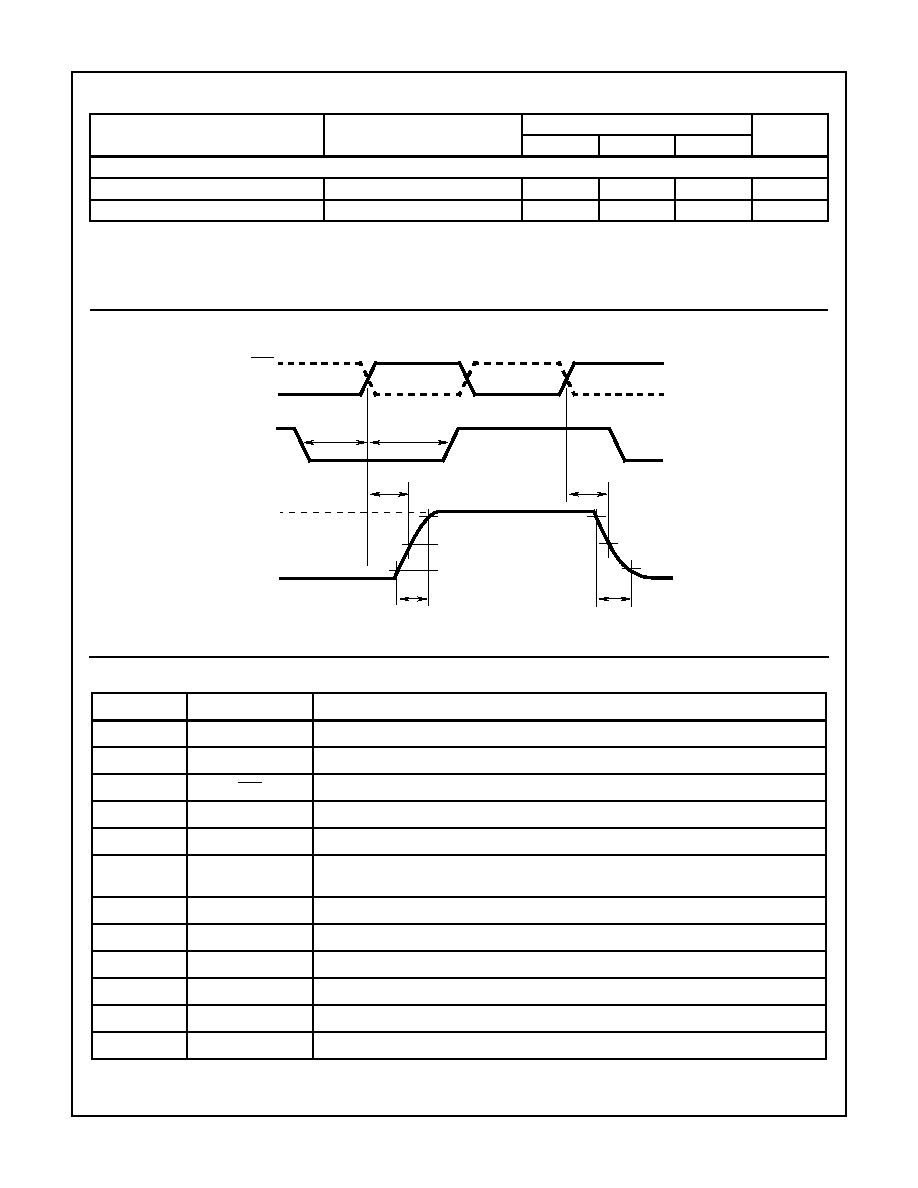
Timing Diagram
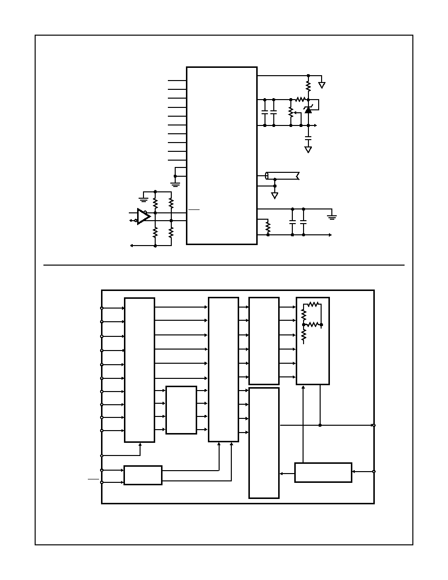
Pin Descriptions
POWER SUPPLY CHARACTERISITICS
I
EE
-60
-75
-90
mA
Power Dissipation
75
load
-
420
470
mW
NOTES:
2. Parameter guaranteed by design or characterization and not production tested.
3. Excludes error due to reference drift.
4. Electrical specifications guaranteed only under the stated operating conditions.
Electrical Specifications
T
A
= 25
o
C, AV
EE
= DV
EE
= -5.2V, AGND = DGND = 0V, R
L
=
, V
OUT
= -1V (Continued)
PARAMETER
TEST CONDITIONS
HI20201JCB/JCP
UNITS
MIN
TYP
MAX
28 PIN SOIC
PIN NAME
PIN DESCRIPTION
1-10
D0 (LSB)-D9 (MSB)
Digital Data Bit 0, the Least Significant Bit thru Digital Data Bit 9, the Most Significant Bit.
11, 12, 19, 21- 25
NC
No Connect, not used.
13
CLK
Negative Differential Clock Input.
14
CLK
Positive Differential Clock Input
15
DV
EE
Digital (ECL) Power Supply -4.75V to -7V.
16
COMPL
Data Complement Pin. When set to a (ECL) logic High the input data is complemented in the
input buffer. When cleared to a (ECL) logic Low the input data is not complemented.
17
DV
SS
Digital Ground.
18
AV
SS
Analog Ground.
20
I
OUT
Current Output Pin.
26
AV
EE
Analog Supply -4.75V to -7V.
27
V
REF
Input Reference Voltage used to set the output full scale range.
28
AV
SS
Analog Ground.
CLK
CLK
DATA
0V
D/A OUT
-1V
90%
50%
10%
N + 1
N + 1
N
t
SU
t
HD
t
D
N
t
r
t
f
t
D
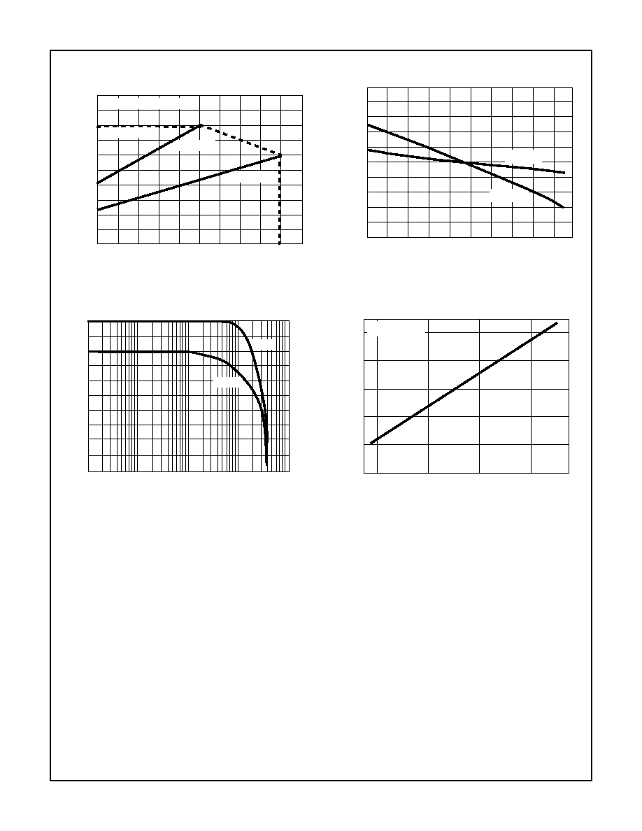
FIGURE 1. LADDER SETTLING TIME FULL POWER BANDWIDTH (LS)
HI20201