
1
CAUTION: These devices are sensitive to electrostatic discharge; follow proper IC Handling Procedures.
1-888-INTERSIL or 321-724-7143
|
Copyright
©
Intersil Corporation 1999
HI2303
Triple 8-Bit, 50 MSPS, Video A/D
Converter with Clamp Function
The HI2303 is a highly integrated 8-bit, 3-channel analog-to-
digital converter that is designed for component (like RGB)
digitizing applications. The internal DC Restore (video
clamp) function and voltage reference simplifies system
design and saves board space. The HI2303 can digitize
RGB, YUV, YIQ and any other analog component color
signals used in video systems. The variety of sub-sampling
modes is compatible with RGB, YUV and YIQ color systems
where 4:4:4, 4:2:2 and 4:1:1 data reduction is needed. The
2-step architecture boasts, low power operation, and
excellent video performance.
Features
∑ Resolution 8-Bit 1/2 LSB (DL)
∑ Low Power Consumption (at 50 MSPS Typ)
(Reference Current Excluded) . . . . . . . . . . . . . . . .500mW
∑ Synchronizing Digital Clamp Function
∑ Clamp ON/OFF Function
∑ Reference Voltage Self-Bias Circuit
∑ Input CMOS/TTL Compatible
∑ Three-State TTL Compatible Output
∑ Single 5V Power Supply or Dual 5V or 3.3V Power Supplies
∑ Low Input Capacitance . . . . . . . . . . . . . . . . . . . . . . . .15pF
∑ Different Digital Output Multiplex Format
- 4:4:4
- 4:2:2
- 4:1:1
∑ Direct Replacement for Sony CXD2303
Applications
∑ Video Digitizing (Composite and Y-C)
∑ LCD Projectors
∑ LCD Panels
∑ RGB Graphics Processing
Pinout
HI2303 (MQFP)
TOP VIEW
Ordering Information
PART NUMBER
TEMP.
RANGE (
o
C)
PACKAGE
PKG. NO.
HI2303JCQ
-40 to 85
80 Ld MQFP
Q80.14x20-S
HI2303EVAL
25
Evaluation Kit
80
79
78
77
75
73
71
69
68
67
65
66
70
72
74
76
64
63
62
61
60
59
58
57
56
55
54
53
52
51
50
49
48
47
46
45
44
43
42
41
2 1
3
4
5
6
7
8
9
10
11
12
13
14
15
16
17
18
19
20
21
22
23
24
26
27
28
29
30
31
32
34
36
38
40
39
37
35
33
25
A5
A0 (LSB)
A1
A2
A3
A4
A6
A7 (MSB)
TGR
DV
DD
DV
SS
C3
AV
DD
C
IO
C
IN
AV
SS
CTL0
XCOE
XBOE
XA
OE
AV
DD
AV
DD
TEST
CTL1
AV
DD
B
IO
B
IN
AV
SS
CLE
REF3
REF2
REF1
CLP
CLK
SEL
SY
CTL2
REF0
TEST
AV
SS
DV
DD
B
RT
B
RBS
B
RTS
A
RTS
A
RT
AV
DD
A
RBS
A
RB
AV
SS
A
IN
A
IO
C
RB
C
RBS
AV
DD
AV
SS
AV
SS
DV
DD
B0 (LSB)
B1
B2
B3
B5
B4
B6
B7 (MSB)
DV
SS
DV
DD
B
RB
C
RT
C
RTS
DV
SS
DV
SS
C0 (LSB)
C1
C2
C4
C5
C6
C7 (MSB)
Data Sheet
December 1998
File Number
4106.2

2
Functional Block Diagram
24
27
38
72
13
20
44
3
10
45
73
80
46
21
30
35
41
42
62
68
22
23
1
2
DV
SS
DV
SS
11
12
71
DV
SS
DV
SS
DV
DD
DV
DD
DV
DD
DV
DD
AV
DD
AV
DD
AV
DD
AV
DD
AV
DD
AV
DD
A0 (LSB)
A7 (MSB)
XAOE
B0 (LSB)
B7 (MSB)
XBOE
C0 (LSB)
C7 (MSB)
XCOE
TGR
TEST
TEST
AV
SS
AV
SS
AV
SS
A-CH
8-BIT ADC
8-BIT
DAC
B-CH
8-BIT ADC
8-BIT
DAC
C-CH
8-BIT ADC
8-BIT
DAC
DIGITAL
CLAMP
CIRCUIT
DIGITAL
CLAMP
CIRCUIT
DIGITAL
CLAMP
CIRCUIT
DATA
SELECTOR
+
LATCH
DIGITAL CONTROL
DECODER
32
31
28
26
25
29
A
IO
A
RBS
A
RB
A
IN
A
RT
A
RTS
8
8
8
8
8
8
33
34
37
39
40
36
B
IO
B
RBS
B
RB
B
IN
B
RT
B
RTS
70
69
66
64
63
67
C
IO
C
RBS
C
RB
C
IN
C
RT
C
RTS
60 61 65
52
58
53
51
54
REF3
REF0
SEL
CLP
CLE
CLK
AV
SS
AV
SS
AV
SS
57
59
43
47
49
50
CTL0
CTL2
SY
48 CTL1
HI2303

3
Pin Description
PIN NO.
SYMBOL
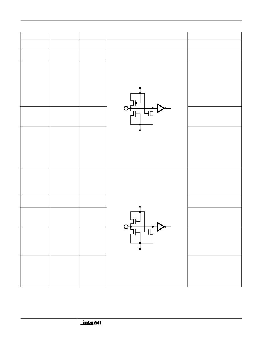
EQUIVALENT CIRCUIT
DESCRIPTION
1, 2, 22, 23
DV
DD
-
Digital Power Supply.
+5V or +3.3V.
13 to 20
3 to 10
73 to 80
A0 to A7
B0 to B7
C0 to C7
O
Digital output.
A0 (LSB) to A7 (MSB)
B0 (LSB) to B7 (MSB)
C0 (LSB) to C7 (MSB).
21
TGR
O
Trigger Output
11, 12, 71, 72
DV
SS
-
Digital Ground.
24, 27, 38, 60, 61,
65
AV
SS
-
Analog Ground.
25
40
63
ARBS
BRBS
CRBS
-
Shorting the RBS pins to AVSS
generates voltage of approxi-
mately 0.6V at the ARB, BRB and
CRB pins.
26
39
64
ARB
BRB
CRB
-
Reference Voltage (Bottom).
31
34
69
ART
BRT
CRT
-
Reference Voltage (Top).
32
33
70
ARTS
BRTS
CRTS
-
Shorting the RTS pins to AV
DD
generates voltage of about 2.5V at
the ART, BRT and CRT pins.
28
37
66
AIN
BIN
CIN
I
Analog Input.
29
36
67
AIO
BIO
CIO
O
Analog Output. These pins are the
D/A
converter
outputs
which
comprise the digital clamp circuit.
DV
DD
DV
SS
31
34
69
32
33
70
26
39
64
25
40
63
AV
DD
RT
RB
R
REF
AV
SS
RTS
RT
RB
RBS
28
37
66
AV
DD
AV
SS
29
36
67
AV
DD
AV
SS
200
HI2303
4
30, 35, 41, 42, 62,
68
AV
DD
Analog +5V Power Supply.
43
59
TEST
I
Normally open. Pull-down
resistors are incorporated.
44
45
46
XAOE
XBOE
XCOE
I
Output Enable Input. When these
pins are Low, data is output from
the digital output pins. When these
pins are High, the digital output
pins are High impedance. The A, B
and C Channels can be controlled
separately. Also, these pins are not
synchronized with the clock signal.
Pull-down
resistors
are
incorporated.
47
48
49
CTL0
CTL1
CLT2
I
Determines
the
digital
output
mode. See the Mode tables and
Timing
Charts.
Pull-down
resistors are incorporated.
50
SY
I
Controls the digital output mode
switching timing. The mode is
switched
by
detecting
the
transition point where this pin
changes from Low to High. See
the Mode Tables and Timing
Charts for details. A pull-down
resister is incorporated.
51
SEL
I
Controls the CLP signal polarity.
When this pin is Low, CLP is High
active.
When this pin is High, CLP is Low
active. This pin has a built-in pull-
down resistor.
52
CLK
I
Clock Input. A pull-down resistor is
incorporated.
53
CLP
I
Clamp Pulse Input. The polarity
can be set to either High or Low by
setting SEL. This pin has a built-in
pull-down resistor.
54
55
56
57
REF0
REF1
REF2
REF3
I
Determines
the
clamp
circuit
reference data. See the mode
tables for the set data. These pins
are not synchronized with the
clock
input
signal.
Pull-down
resistors are incorporated.
58
CLE
I
Clamp Enable. When this pin is Low
the clamp circuit does not operate.
When this pin is High, the clamp
circuit
operates.
A
pull-down
resistor is incorporated.
Pin Description
(Continued)
PIN NO.
SYMBOL
EQUIVALENT CIRCUIT
DESCRIPTION
AV
DD
AV
SS
AV
DD
AV
SS
HI2303

5
Absolute Maximum Ratings
T
A
= 25
o
C
Thermal Information
Supply Voltage (AV
DD
, DV
DD
) . . . . . . . . . . . . . . . . . . . . . . . . . . . .7V
Input Voltage (V
IN
, All Pins). . . . . . . . . . . . V
DD
+0.5V to V
SS
-0.5V
Output Voltage (V
D
, Digital) . . . . . . . . . . . . V
DD
+0.5V to V
SS
-0.5V
Operating Conditions
Supply Voltage:
AV
DD
, AV
SS
. . . . . . . . . . . . . . . . . . . . . . . . . . . . . . 4.75V to 5.25V
DV
DD
, DV
SS
. . . . . . . . . . . . . . . . . . . . . . . . . . . . . . . . 3.0V to 5.5V
|
DV
SS
, AV
SS
| . . . . . . . . . . . . . . . . . . . . . . . . . . . . . 0mV to 100mV
Reference Input Voltage:
V
ARB
, V
BRB
, V
CRB
. . . . . . . . . . . . . . . . . . . . . . . . . . . 0V or More
V
ART
, V
BRT
, V
CRT
. . . . . . . . . . . . . . . . . . . . . . . . . . .2.7V or Less
Analog Input:
A
IN
, B
IN
, C
IN
. . . . . . . . . . . . . . . . . . . . . . . . . . . .1.7V
P-P
or More
Clock Pulse Width:
t
PW1
, t
PW0
. . . . . . . . . . . . . . . . . . . . . . . . . 9ns (Min) to 1.1ms (Max)
Ambient Temperature (TOPR) . . . . . . . . . . . . . . . . . . -40
o
C to 85
o
C
Thermal Resistance (Typical, Note 1)
JA
(
o
C/W)
MQFP Package . . . . . . . . . . . . . . . . . . . . . . . . . . . .
88
Maximum Junction Temperature (Plastic Package) . . . . . . . .150
o
C
Maximum Storage Temperature Range (T
STG
). . . . -65
o
C to 150
o
C
Maximum Lead Temperature (Soldering 10s) . . . . . . . . . . . . .300
o
C
(Lead Tips Only)
CAUTION: Stresses above those listed in "Absolute Maximum Ratings" may cause permanent damage to the device. This is a stress only rating and operation of the
device at these or any other conditions above those indicated in the operational sections of this specification is not implied.
NOTE:
1.
JA
is measured with the component mounted on an evaluation PC board in free air.
Electrical Specifications
f
C
= 50 MSPS, AV
DD
= 5V, DV
DD
= 3.0V to 5.0V, V
RB
= 0.5V, V
RT
= 2.5V, T
A
= 25
o
C
PARAMETER
SYMBOL
TEST CONDITIONS
MIN
TYP
MAX
UNITS
ANALOG CHARACTERISTICS
DV
DD
= 3V to 5.5V
Conversion Rate
f
C
AV
DD
= 4.75V to 5.25V, T
A
= -20
o
C to 75
o
C,
V
IN
= 0.5V to 2.5V, f
IN
= 1kHz Triangular Wave
0.5
-
50
MSPS
Analog Input Band (-1dB)
BW
Envelope
-1dB
-
60
-
MHz
R
IN
= 33
-3dB
-
100
-
MHz
Differential Non-Linearity Error
E
D
End Point
-
±
0.3
±
0.5
LSB
Integral Non-Linearity Error
E
L
-
±
0.7
±
1.5
LSB
Offset Voltage (Note 2)
E
OT
Potential Difference to A
RT
, B
RT
, C
RT
-50
-
-10
mV
E
OB
Potential Difference to A
RB
, B
RB
, C
RB
0
-
40
mV
Differential Gain Error
DG
NTSC 40 IRE Mod Ramp, f
C
= 14.3 MSPS
-
3
-
%
Differential Phase Error
DP
-
1.5
-
Deg
Cross Talk
CT
f
IN
= 1MHz Sinewave
-
52
-
dB
Clamp Offset Voltage
E
OC
V
IN
= DC
C
IN
= 10
µ
F
t
PCW
= 2.75
µ
s
f
CLK
= 14.3MHz
f
CLP
= 15.75kHz
Ref Data = 00010000
-
-
±
1
LSB
Ref Data = 10000000
-
-
±
1
LSB
Signal To Noise Ratio
SNR
f
IN
= 150kHz
-
43
-
dB
f
IN
= 500kHz
-
42
-
dB
f
IN
= 1MHz
-
42
-
dB
f
IN
= 3MHz
-
41
-
dB
f
IN
= 10MHz
-
38
-
dB
f
IN
= 20MHz
-
35
-
dB
HI2303