10-1
Semiconductor
August 1997
HI2304
Triple 8-Bit, 20 MSPS, RGB,
3-Channel D/A Converter
Features
∑ Resolution . . . . . . . . . . . . . . . . . . . . . . . . . . . Triple 8-Bit
∑ Maximum Conversion Speed . . . . . . . . . . . . . . . 20MHz
∑ RGB 3-Channel Input/Output
∑ Differential Linearity Error . . . . . . . . . . . . . . .
±
0.5 LSB
∑ Low Power Consumption . . . . . . . . . . . . . . . . . . .50mW
(330
Load for 1.2V
P-P
Output)
∑ Single Power Supply . . . . . . . . . . . . . . . . . . . . . . . +3.3V
∑ Low Glitch Noise
∑ Direct Replacement for Sony CXD2304
Applications
∑ Digital TV
∑ Graphics Display
∑ High Resolution Color Graphics
∑ Video Reconstruction
∑ Instrumentation
∑ Image Processing
∑ I/Q Modulation
Description
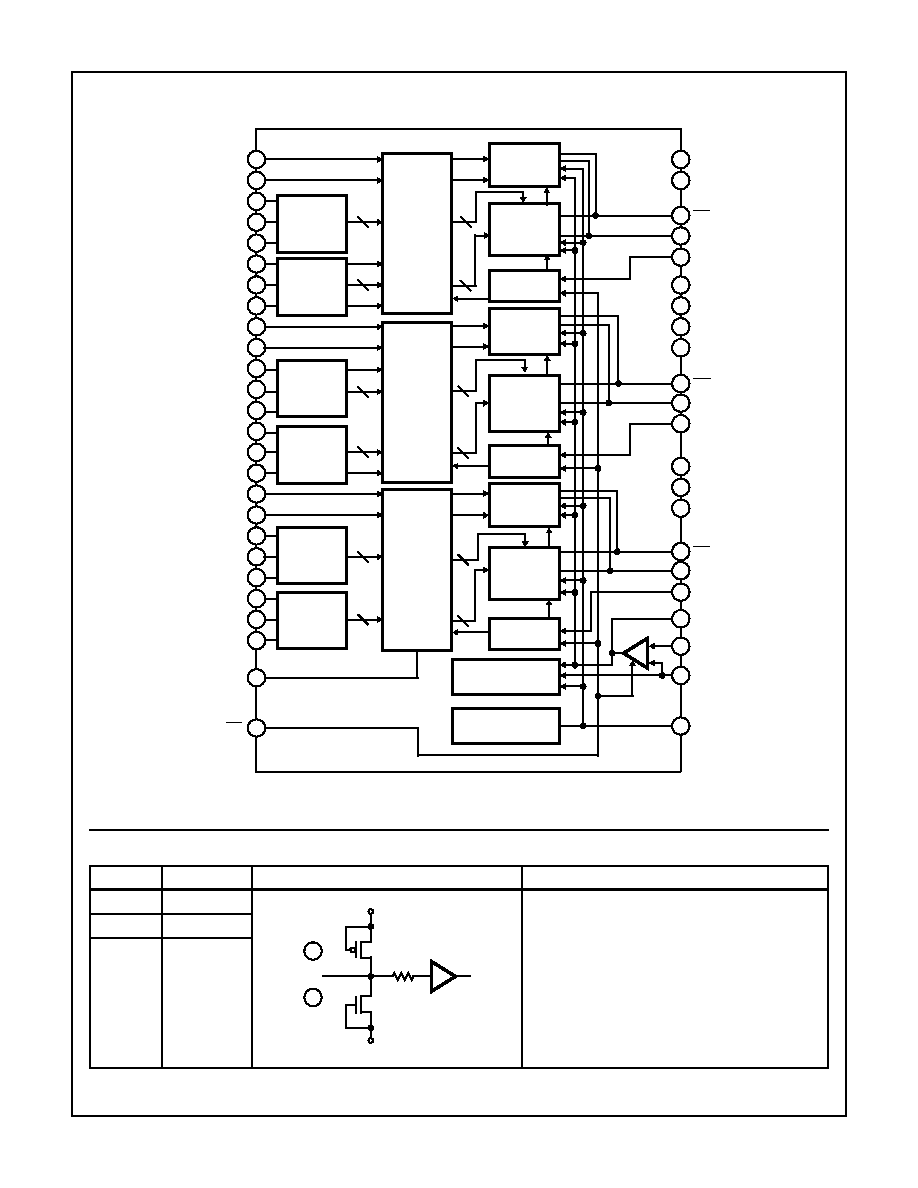
The HI2304 is a triple 8-bit, high-speed, CMOS D/A
converter designed for video band use. It has three
separate, 8-bit, pixel inputs, one each for red, green, and
blue video data. A single 3.3V power supply and pixel clock
input can be controlled individually, or connected together
as one. The HI2304 also has BLANK video control signal.
For faster speed and 5.0V operation, refer to the HI1178.
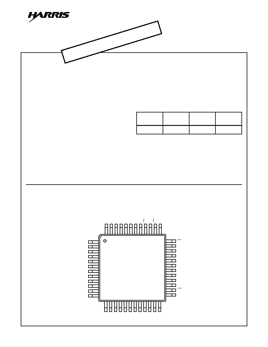
Pinout
HI2304
(MQFP)
TOP VIEW
Ordering Information
PART
NUMBER
TEMP.
RANGE (
o
C)
PACKAGE
PKG. NO.
HI2304JCQ
-20 to 75
48 Ld MQFP
Q48.7x7-S
1
2
3
4
5
6
7
8
32
31
30
29
28
27
26
25
24
23
22
21
20
19
18
17
9
10
11
12
13 14 15 16
33
34
35
36
37
38
39
40
41
42
43
44
45
46
47
48
R0
I
REF
V
REF
AV
SS
VB
DV
SS
DV
SS
BCK
GCK
RCK
CE
BLK
R0
R1
R2
R3
R4
R7
G0
G1
G2
G3
R5
R6
DV
DD
DV
DD
AV
DD
AV
DD
AV
DD
VG
B0
B0
G0
G0
R0
AV
DD
G4
G5
G6
G7
B0
B1
B2
B3
B4
B5
B6
B7
CAUTION: These devices are sensitive to electrostatic discharge. Users should follow proper IC Handling Procedures.
Copyright
©
Harris Corporation 1997
File Number
4116.1
NOT RECOMMENDED FOR NEW DESIGNS
See HI1178

10-4
35
I
REF
Connect a resistance 16 times "16R" that of output
resistance value "R".
34
V
REF
Set full scale output value.
42
VG
Connect a capacitor of about 0.1
µ
F.
43 to 46
AV
DD
Analog V
DD
.
37
RO
Current output pin. Voltage output can be obtained by
connecting a resistance.
39
GO
41
BO
36
RO
Inverted current output pin. Normally dropped to analog
GND.
38
GO
40
BO
47, 48
DV
DD
Digital V
DD
.
Pin Descriptions
(Continued)
PIN NO.
SYMBOL
EQUIVALENT CIRCUIT
DESCRIPTION
35
34
42
AV
SS
AV
SS
AV
SS
AV
DD
AV
DD
AV
DD
AV
DD
-
+
37
39
41
36
38
40
AV
SS
AV
SS
AV
DD
AV
DD
HI2304
10-5
I/O Chart
(When Full Scale Output Voltage at 2.00V)
Absolute Maximum Ratings
T
A
= 25
o
C
Thermal Information
Supply Voltage (V
DD
) . . . . . . . . . . . . . . . . . . . . . . . . . . . . . . . . . . 7V
Input Voltage (V
IN
) . . . . . . . . . . . . . . . . . . . . . . . . . . . . . V
DD
to V
SS
Output Current (I
OUT
). . . . . . . . . . . . . . . . . . . . . . . . . .0mA to 15mA
(Every Each Channel)
Operating Conditions
Temperature Range (T
OPR
) . . . . . . . . . . . . . . . . . . . . -20
o
C to 75
o
C
Supply Voltage
AV
DD
, AV
SS
. . . . . . . . . . . . . . . . . . . . . . . . . . . . . . . .3.0V to 3.6V
DV
DD
, DV
SS
. . . . . . . . . . . . . . . . . . . . . . . . . . . . . . . .3.0V to 3.6V
Reference Input Voltage (V
REF
) . . . . . . . . . . . . . . . . . . . . . . . . 1.2V
Clock Pulse Width
t
PW1
. . . . . . . . . . . . . . . . . . . . . . . . . . . . . . . . . . . . . . . 25ns (Min)
t
PW0
. . . . . . . . . . . . . . . . . . . . . . . . . . . . . . . . . . . . . . . 25ns (Min)
Thermal Resistance (Typical, Note 1)
JA
(
o
C/W)
MQFP Package . . . . . . . . . . . . . . . . . . . . . . . . . . . .
104
Maximum Junction Temperature (Plastic Package) . . . . . . . . 150
o
C
Maximum Storage Temperature (T
STG
) . . . . . . . . . .-65
o
C to 150
o
C
Maximum Lead Temperature (Soldering 10s) . . . . . . . . . . . . . 300
o
C
(Lead Tips Only)
CAUTION: Stresses above those listed in "Absolute Maximum Ratings" may cause permanent damage to the device. This is a stress only rating and operation of
the device at these or any other conditions above those indicated in the operational sections of this specification is not implied.
NOTE:
1.
JA
is measured with the component mounted on an evaluation PC board in free air.
Electrical Specifications
f
CLK
= 20MHz, V
DD
= 3.3V, R
OUT
= 330
, V
REF
= 1.2V, R
IRF
= 5.1k
, T
A
= 25
o
C
PARAMETER
SYMBOL
TEST CONDITIONS
MIN
TYP
MAX
UNITS
Resolution
n
-
8
-
Bit
Maximum Conversion Speed
f
MAX
20
-
-
MHz
Linearity Error
INL
-2.5
-
2.5
LSB
Differential Linearity Error
DNL
-0.5
-
0.5
LSB
Full Scale Output Voltage
V
FS
1.12
1.24
1.36
V
Full Scale Output Ratio (Note 1)
F
SR
0
1.5
3
%
Full Scale Output Current
I
FS
-
3.8
-
mA
Offset Output Voltage
V
OS
-
-
1
mV
Power supply Current
I
DD
14.3MHz, at Color Bar Data input
-
15
-
mA
Digital Input
Current
H Level
I
IH
-
-
5
µ
A
L Level
I
IL
-5
-
-
µ
A
Set Up Time
t
S
7
-
-
ns
Hold Time
t
H
3
-
-
ns
Propagation Delay Time
t
PD
-
20
-
ns
Glitch Energy
GE
-
150
-
pV/s
Crosstalk
CT
1MHz Sine Wave Output
-
53
-
dB
NOTE:
2. Full Scale Output Ratio =
x 100(%).
INPUT CODE
OUTPUT VOLTAGE
MSB
LSB
1
1
1
1
1
1
1
1
1.2V
∑
∑
∑
1
0
0
0
0
0
0
0
0.6V
∑
∑
∑
0
0
0
0
0
0
0
0
0V
Full scale voltage of channel
Average of the full-scale voltage of the channels
-------------------------------------------------------------------------------------------------------------------------------
1
≠
HI2304