10-1
Æ
August 1997
HI2307
Triple 10-Bit, 50 MSPS,
RGB, 3-Channel D/A Converter
Features
∑ Resolution . . . . . . . . . . . . . . . . . . . . . . . . . .Triple 10-Bit
∑ Maximum Conversion Speed . . . . . . . . . . . . . . . 50MHz
∑ RGB 3-Channel Input/Output
∑ Differential Linearity Error . . . . . . . . . . . . . . .
±0.5 LSB
∑ Low Power Consumption . . . . . . . . . . . . .300mW (Max)
∑ Single Power Supply . . . . . . . . . . . . . . . . . . . . . . . . . +5V
∑ Low Glitch
∑ Direct Replacement for Sony CXD2307
Applications
∑ Digital TV
∑ Graphics Display
∑ High Resolution Color Graphics
∑ Video Reconstruction
∑ Instrumentation
∑ Image Processing
∑ I/Q Modulation
Description
The HI2307 is a triple 10-bit, high-speed, CMOS D/A
converter designed for video band use. It has three sepa-
rate, 10-bit, pixel inputs, one each for red, green, and blue
video data. A single 5.0V power supply and pixel clock input
is all that is required to make the device operational. A bias
voltage generator is internal. Each channel clock input can
be controlled individually, or connected together as one. The
HI2307 also has BLANK video control signal.
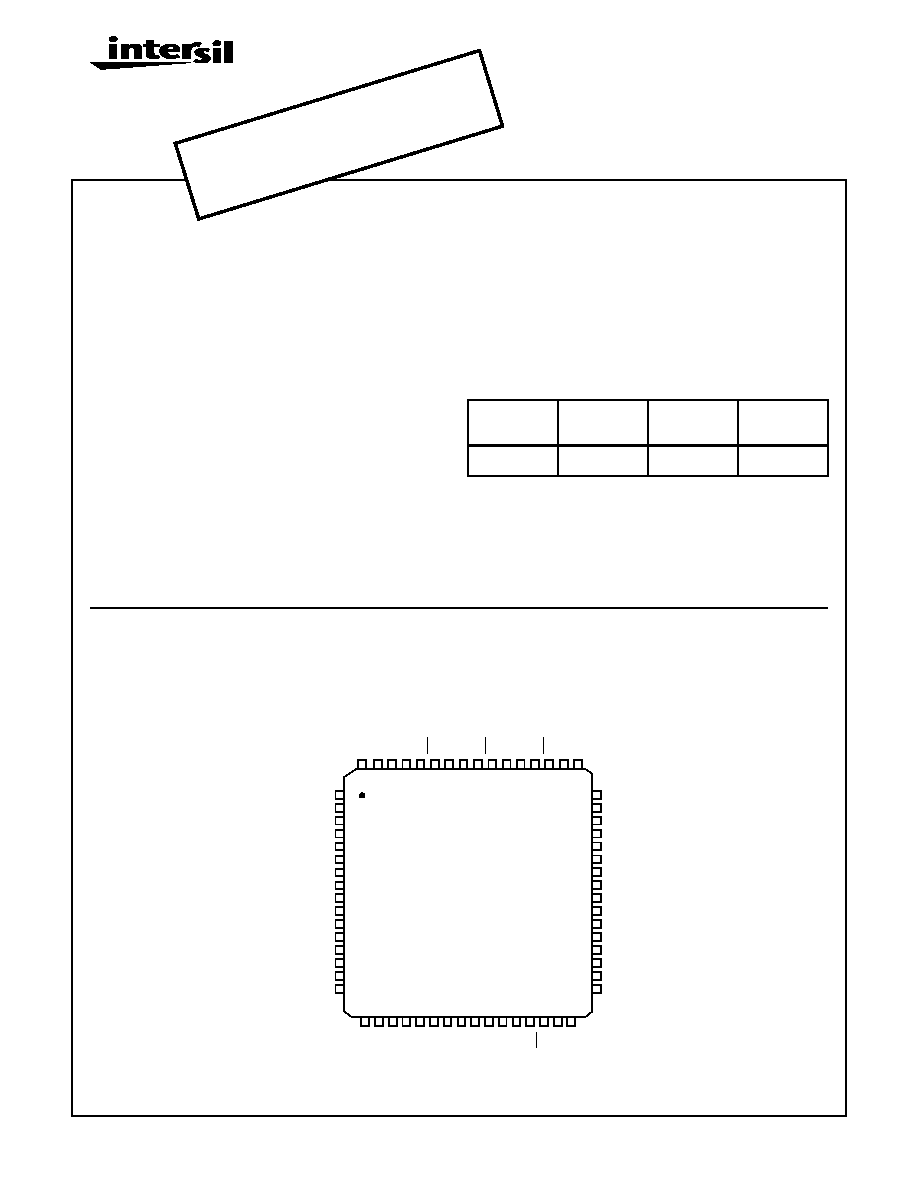
Pinout
HI2307
(MQFP)
TOP VIEW
Ordering Information
PART
NUMBER
TEMP.
RANGE (
o
C)
PACKAGE
PKG. NO.
HI2307JCQ
-20 to 75
64 Ld MQFP
Q64.10x10-S
6463 62 61 60 59 58 57 56 55 54 53 52 51 50 49
17 18 19 20 21 22 23 24 25 26 27 28 29 30 31 32
1
2
3
4
5
6
7
8
9
10
11
12
13
14
15
16
R1
RO
(
L
S
B
)
DV
DD
AV
DD
AV
DD
BO
BO
AV
DD
AV
DD
GO
GO
AV
DD
AV
DD
RO
RO
AV
SS
G8
G9
B1
B0
(
L
S
B
)
B2
B3
B4
B5
B6
B7
B8
RCK
BL
K
CE
B9
GC
K
48
47
46
45
44
43
42
41
40
39
38
37
36
35
34
33
VGB
ROB
VGG
ROG
VGR
ROR
VRB
VRG
VRR
IRB
IRG
IRR
AV
SS
VB
DV
SS
BCK
R2
R3
R4
R5
R6
R7
R8
R9
G0 (LSB)
G1
G2
G3
G4
G5
G6
G7
CAUTION: These devices are sensitive to electrostatic discharge; follow proper IC Handling Procedures.
1-888-INTERSIL or 321-724-7143
|
Intersil (and design) is a registered trademark of Intersil Americas Inc.
Copyright © Intersil Americas Inc. 2002. All Rights Reserved
File Number
4117.1
NOT
REC
OMM
END
ED F
OR N
EW D
ESIG
NS
See
HI30
50
or co
ntac
t our
Tec
hnic
al Su
ppor
t Cen
ter a
t
1-88
8-INT
ERS
IL or
www
.inte
rsil.c
om/t
sc

10-4
43
45
47
ROR
ROG
ROB
Connect to VGR, VGG, and VGB with the control
method of output amplitude. See Application
Circuit.
44
46
48
VGR
VGG
VGB
Connect a capacitor of approximately 0.1
µF.
37
38
39
IRR
IRG
IRB
Connect to AV
SS
with a resistance of 3.3k
.
40
41
42
VRR
VRG
VRB
Set output fullscale value (2.0V).
50
RO
Current output pins. Output can be retrieved by
connecting a resistance of 200
to AV
SS
.
54
GO
58
BO
51
RO
Reverse current output pins. Normally connect to
AV
SS
.
55
GO
59
BO
62
DV
DD
Digital V
DD
.
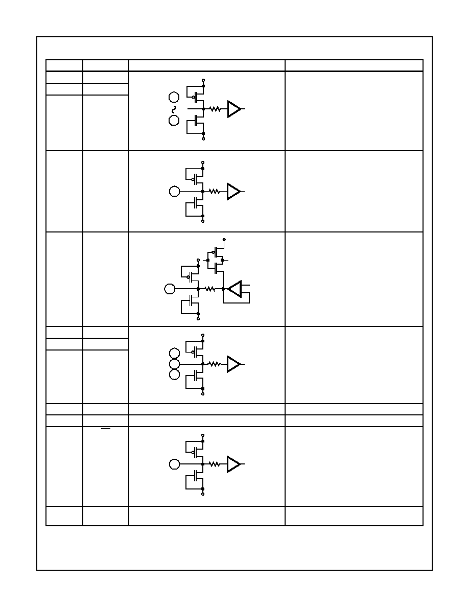
Pin Descriptions
(Continued)
NUMBER
SYMBOL
EQUIVALENT CIRCUIT
DESCRIPTION
45
AV
DD
AV
SS
47
43
46
AV
DD
AV
SS
48
44
38
AV
DD
AV
SS
39
37
-
+
41
AV
DD
AV
SS
42
40
54
AV
DD
AV
SS
58
50
55
AV
DD
AV
SS
59
51
HI2307

10-5
Absolute Maximum Ratings
T
A
= 25
o
C
Thermal Information
Supply Voltage, V
DD
. . . . . . . . . . . . . . . . . . . . . . . . . . . . . . . . . 7.0V
Input Voltage, V
IN
. . . . . . . . . . . . . . . . . . . . . . . . . . . . . . V
DD
to V
SS
Output Current (for Each Channel), l
OUT
. . . . . . . . . . . . . 0 to 15mA
Operating Conditions
Supply Voltage
AV
DD
, AV
SS
. . . . . . . . . . . . . . . . . . . . . . . . . . . . . .4.75V to 5.25V
DV
DD
, DV
SS
. . . . . . . . . . . . . . . . . . . . . . . . . . . . . .4.75V to 5.25V
Reference Input Voltage, V
REF
. . . . . . . . . . . . . . . . . . .0.5V to 2.0V
Clock Pulse Width
t
PW1
. . . . . . . . . . . . . . . . . . . . . . . . . . . . . . . . . . . . . . . 10ns (Min)
t
PW0
. . . . . . . . . . . . . . . . . . . . . . . . . . . . . . . . . . . . . . . 10ns (Min)
Temperature Range, T
OPR
. . . . . . . . . . . . . . . . . . . . -20
o
C to 75
o
C
Thermal Resistance (Typical, Note 7)
JA
(
o
C/W)
MQFP Package . . . . . . . . . . . . . . . . . . . . . . . . . . . .
93
Maximum Junction Temperature (Plastic Package) . . . . . . . . 150
o
C
Maximum Storage Temperature Range . . . . . . . . . . -65
o
C to 150
o
C
Maximum Lead Temperature (Soldering 10s). . . . . . . . . . . . . 300
o
C
(Lead Tips Only)
CAUTION: Stresses above those listed in "Absolute Maximum Ratings" may cause permanent damage to the device. This is a stress only rating and operation
of the device at these or any other conditions above those indicated in the operational sections of this specification is not implied.
NOTE:
1.
JA
is measured with the component mounted on an evaluation PC board in free air.
Electrical Specifications
T
A
= 25
o
C, f
CLK
= 50MHz, V
DD
= 5V, R
OUT
= 200
, V
REF
= 2.0V
PARAMETER
SYMBOL
TEST CONDITIONS
MIN
TYP
MAX
UNITS
Resolution
n
-
10
-
Bit
Maximum Conversion Speed
f
MAX
50
-
-
MHz
Linearity Error
E
L
-2.0
-
2.0
LSB
Differential Linearity Error
E
D
-0.5
-
0.5
LSB
Output Full Scale Voltage
V
FS
1.8
1.9
2.0
V
Output Full Scale Ratio (Note 8)
F
SR
For the Equal Gain
0
1.5
3
%
Output Full Scale Current
I
FS
-
9.5
10
mA
Output Offset Voltage
V
OS
-
-
1
mV
Supply Current
I
DD
-
55
60
mA
Digital Input
Current
High Level
I
IH
-
-
5
µA
Low Level
I
IL
-5
-
-
µA
Precision Guaranteed Output Voltage
Range
V
OC
1.8
1.9
2.0
V
Setup Time
t
S
-
5
7
ns
Hold Time
t
H
-
1
3
ns
Propagation Delay Time
t
PD
-
10
-
ns
Glitch Energy
GE
-
100
-
pV-s
Cross Talk
CT
For 10MHz Sinewave Output
-
54
-
dB
NOTE:
2. Output Full Scale Ratio =
.
Full scale voltage of channel
Average of the full scale voltage of the channels
------------------------------------------------------------------------------------------------------------------------------- 1
≠
( ) x100(%)
HI2307