 | ÐлекÑÑоннÑй компоненÑ: HI2570JCQ | СкаÑаÑÑ:  PDF PDF  ZIP ZIP |
Äîêóìåíòàöèÿ è îïèñàíèÿ www.docs.chipfind.ru
1
®
September 1997
HI2570, CXD2570
1-Bit AD/DA
Converter For Audio Application
Features
· Two-Channel AD/DA Converters and Their Each Deci-
mation and Oversampling Digital Filter in a Single Chip
· Simplified External Parts with a Built-In Analog Circuit
Around AD Converter
· Distortion
- ADC . . . . . . . . . . . . . . . . . . . . . . . . . . . . . . . . . . 0.015%
- DAC . . . . . . . . . . . . . . . . . . . . . . . . . . . . 0.009% (-3dB)
· S/N Ratio (Typical Values when F
S
= 16kHz)
- ADC . . . . . . . . . . . . . . . . . . . . . . . . . . . . . . . . . . . .80dB
- DAC . . . . . . . . . . . . . . . . . . . . . . . . . . . . . . . . . . . .90dB
· Ripple in the Digital Filter Pass Band
. . . . . . . ±0.05dB<
· Attenuation in the Digital Filter Rejection Band. . . 45dB>
Applications
- Telephones, TV Conference Systems, Language Lab-
oratory Equipment, TV Game Equipment and Elec-
tronic Musical Instrument
Description
The HI2570, CXD2570 is a 1-bit stereo AD/DA converter
which uses a 2nd-order
system noise shaper. This LSI is
especially suited for sampling frequency between 8kHz and
32kHz.
Function
· Data Can Be Input/Output at Rate of 1xF
S
with a Built-
In Digital Filter
· Multi-Channel Systems can be Connected Using Several
HI2570, CXD2570Qs
· The 32-Slot Serial Data Interface Enables Independent
Selection of Data Frontward Truncation/Rearward
Truncation and MSB First/LSB First
· 512F
S
/1024F
S
(when F
S
= 8 to 16kHz) or 256F
S
/512F
S
/
768F
S
/1024F
S
(When F
S
= 16 to 32kHz) Can be Used
as the Master Clock
· The Sampling Frequency of Not Only 8kHz or 16kHz, but
32kHz or 44.1kHz Can Be Used for Audio Equipment
· Various Frequency Divided Clocks are Output for LSIs
Connected
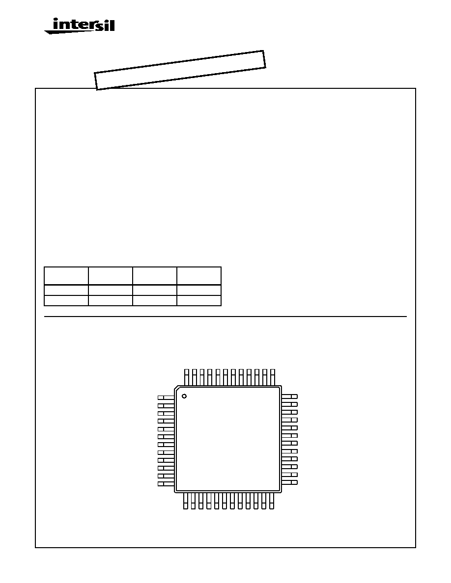
Pinout
HI2570, CXD2570 (48 LEAD MQFP)
TOP VIEW
Ordering Information
PART
NUMBER
TEMP.
RANGE (
o
C)
PACKAGE
PKG. NO.
HI2570JCQ
-20 to 55
48 Ld MPQF
Q48.12x12-S
CXD2570Q
-20 to 55
48 Ld MPQF
Q48.12x12-S
1
2
3
4
5
6
7
8
32
31
30
29
28
27
26
25
24
23
22
21
20
19
18
17
9
10
11
12
13 14 15 16
33
34
35
36
37
38
39
40
41
42
43
44
45
46
47
48
XSL2
XSL1
XSL0
MLSL
MASL
DV
SS
SOUT
SIN
BCK
LRCK
MS
DV
DD
AV
DD
3
AOUT1-
AV
SS
3
UCLK
XCLK
XTLO
XV
SS
AV
SS
4
AOUT2-
AV
DD
4
XV
DD
XTLI
AO
UT
1
+
AV
SS
3
AV
SS
1
AIN1
AV
DD
1
NC
NC
DV
DD
WO
DAS
L
1
DAS
L
0
SU
B
AO
UT
2
+
AV
SS
4
AV
SS
2
AIN2
AV
DD
2
NC
SU
B
NC
DV
SS
X
M
CK2
TE
S
T
CL
R
CAUTION: These devices are sensitive to electrostatic discharge; follow proper IC Handling Procedures.
1-888-INTERSIL or 321-724-7143
|
Intersil (and design) is a registered trademark of Intersil Americas Inc.
Copyright © Intersil Americas Inc. 2002. All Rights Reserved
File Number
4122.1
NOT REC
OMMEND
ED FOR N
EW DESIG
NS

2
®
File Number
3
Pin Descriptions
PIN NO.
SYMBOL
I/O
DESCRIPTION
1
AV
DD
3
--
Analog power supply for channel-1 DA converter
2
AOUT1 (-)
O
Analog reversed phase output of channel-1 DA converter
3
AV
SS
3
--
Analog GND for channel-1 DA converter
4
UCLK
O
Outputs a 1/2 frequency divider of clock input from oscillation pin XTLI (Pin 7).
User clock output for the externally connected ICs.
5
XCLK
O
256Fs/512Fs clock output. This provides the master clock for ICs operating in
the slave mode when multiple CXD2570Qs are connected.
6
XV
DD
--
Digital power supply for the master clock
7
XTLI
I
Crystal oscillation circuit input. Connects the crystal oscillator selected by the
crystal selector pins XSL0 to 2 (Pins 34, 35 and 36). To input an external mas-
ter clock, this pin is used.
8
XTLO
O
Crystal oscillation circuit output. Connects the crystal oscillator selected by the
crystal selector pins XSL0 to 2 (Pins 34, 35 and 36).
9
XV
SS
--
Digital GND for the master clock
10
AV
SS
4
--
Analog GND for channel-2 DA converter
11
AOUT2 (-)
O
Analog reversed phase output of channel-2 DA converter
12
AV
DD
4
--
Analog power supply for channel-2 DA converter
13
AOUT2 (+)
O
Analog forward phase output of channel-2 DA converter
14
AV
SS
4
--
Analog GND for channel-2 DA converter
15
AV
SS
2
--
Analog GND for channel-2 AD converter
16
AIN1
I
Analog input of channel-2 converter
17
AV
DD
2
--
Analog power supply for channel-2 AD converter
18
NC
--
19
SUB
--
Connected to the substrate in the IC (having the same potential as power sup-
ply). Connect this pin to GND via a capacitor on the external printed wiring
board.
20
NC
--
21
DV
SS
--
Digital GND
22
XMCK2
O
IC measurement. Normally, Low is output.
23
TEST
I
Test. Normally, fixed at Low. Equipped with a pull-down resistor.
24
CLR
I
System clear input. Normally, fixed at High; cleared at Low. Equipped with a
pull-up resistor.
25
DV
DD
--
Digital power supply.
26
MS
I
Master/slave mode switching input. High = Master mode. Low = Slave mode.
Equipped with a pull-up resistor.
27
LRCK
I/O
Sampling frequency clock pin of serial I/O. Outputs in master mode (when Pin
26 is High). Inputs in slave mode (when Pin 26 is Low). Transfers channel-1
data at High; transfers channel-2 data at Low.
HI2570, CXD2570

4
28
BCK
I/O
Serial bit transfer clock for serial input data SIN or serial output data SOUT
(64FS). Outputs in master mode (when Pin 26 is High). Inputs in slave mode
(when Pin 26 is Low). Retrieves serial input data at
; send serial out-
put data at
.
29
SIN
I
Serial data input of 2-channel sampling. The data format is 2's complement,
and consists of 32-bit slot.
30
SOUT
O
Serial data output of 2-channel per sampling. The data format is 2's comple-
ment, and consists of 32-bit slot.
31
DV
SS
--
Digital GND
32
MASL
I
Selects whether 16-bit serial data is applied in the first 16-bits or the last 16-
bit of 32-bit slot in serial I/O. High = Frontward truncation; Low = Rearward
truncation
33
MLSL
I
Selects whether 16-bit serial data is input/output at LSB first or MSB first in
serial I/O. High = MSB first; Low = LSB first
34
XSL0
I
Crystal oscillator selection. Three bits, XSL0 to 2. Selects the clock frequency
to be input from XTLI (Pin 7).
35
XSL1
I
Crystal oscillator selection. Three bits, XSL0 to 2. Selects the clock frequency
to be input from XTLI (Pin 7).
36
XSL2
I
Crystal oscillator selection. Three bits, XSL0 to 2. Selects the clock frequency
to be input from XTLI (Pin 7).
37
DASL0
I
IC measurement. Normally, fixed at High.
38
DASL1
I
IC measurement. Normally fixed at Low.
39
WO
I
Window masked when High; window open when Low (forced synchroniza-
tion). Equipped with a pull-up resistor.
40
DV
DD
--
Digital power supply
41
NC
--
42
NC
--
43
SUB
--
Connected to the substrate in the IC (having the same potential as power sup-
ply). Connect this pin to GND via capacitor on the external printed wiring
board.
44
AV
DD
1
--
Analog power supply for channel-1 AD converter
45
AIN1
I
Analog input of channel-1 AD converter
46
AV
SS
1
--
Analog GND for channel-1 AD converter
47
AV
SS
3
--
Analog GND for channel-1 DA converter
48
AOUT1 (+)
O
Analog forward phase output of channel-1 DA converter
Pin Descriptions
(Continued)
PIN NO.
SYMBOL
I/O
DESCRIPTION
HI2570, CXD2570
5
Absolute Maximum Ratings
T
A
= 25
o
C
I/O Capacitance
Supply Voltage (V
DD
). . . . . . . . . . . . . . . . . . . . . . V
SS
0.5V to 7.0V
Input Voltage (V
1
). . . . . . . . . . . . . . . . . . .V
SS
0.5V to V
DD
+ 0.5V
Output Voltage (V
0
) . . . . . . . . . . . . . . . . . V
SS
0.5V to V
DD
+ 0.5V
Operating Temperature (Topr) . . . . . . . . . . . . . . . . . . -20
o
C to 75
C
Storage Temperature (Tstg . . . . . . . . . . . . . . . . . . . -55
o
C to 150
o
C
Recommended Operating Conditions
. . . . . . . . . . . . . . . . . . . . . . . . . . . . . . . . . . . MIN
TYP
MAX
Supply Voltage (Note 1) (V
DD
)
4.5V
5.0V
5.5V
Ambient Temperature (T
A
) . . . . . . . . . . . . . . -20
o
C
--
+75
o
C
Sampling Frequency (Note 2) (F
S
). . . . . . . . 7kHz
--
33kHz
. . . . . . . . . . . . . . . . . . . . . . . . . . . . . . . . . . MIN
TYP
MAX
Input Pin (C
IN
)
. --
--
9pF
Output Pin (C
OUT
) . . . . . . . . . . . . . . . . . . .
--
--
11pF
Bidirectional Pin (C
I/O
) . . . . . . . . . . . . . . . . ---
--
11 pF
Measurement conditions: V
DD
= V
1
= 0V, f = 1MHz
CAUTION: Stresses above those listed in "Absolute Maximum Ratings" may cause permanent damage to the device. This is a stress only rating and operation
of the device at these or any other conditions above those indicated in the operational sections of this specification is not implied.
NOTES:
1. The analog power supplies for AD converters (Pins 17 and 44) must be turned on simultaneously with or before other poser supplies.
turning on these power supplies after any other power supply may cause the device to fall into latch-up condition. this precaution, how-
ever, does not apply when turning off the power supplies.
2. Although the device can operate with F
S
frequencies such as F
S
= 44.1kHz or 48kHz, its analog characteristics deteriorate to extent.
When used at only these F
S
frequencies, the CXD255Q is recommended that is pin-compatible with the CXD2570Q.
Electrical Specifications
PARAMETER
SYMBOL
TEST
CONDITIONS
PART NUMBER
OR GRADE
UNITS
APPLICABLE
PINS
MIN
TYP
MAX
DC Characteristics
AV
DD
1 = AV
DD
2 = AV
DD
3 = AV
DD
4 = XV
DD
= DV
DD
= 5.0V ± 10%, AV
SS
1 = AV
SS
2 = AV
SS
3 = AV
SS
4 =
XV
SS
= DV
SS
= 0V, T
A
= -20
o
C to 75
o
C
Input Voltage
V
IHC
0.7V
DD
--
--
V
*1
V
ILC
Ò
Ò
0.3V
DD
V
IN
Analog Input
V
SS
--
V
DD
V
*2
Output Voltage
V
OH1
I
OH
= -2mA
V
DD
-0.5
--
V
DD
V
*3
V
OL1
I
OL
= 4mA
0
--
0.4
V
OH2
I
OH
= -4mA
V
DD
-0.5
--
V
DD
V
*4
V
OL2
I
OL
= 4mA
0
--
0.4
V
OH3
I
OH
= -12mA
V
DD
/2
--
V
DD
V
*5
V
OL3
I
OL
= 16mA
0
--
V
DD
/2
V
OH4
I
OH
= -2mA
V
DD
-0.8
--
V
DD
V
*6
V
OL4
I
OL
= 4mA
0
--
0.4
Input Leak Current 1
I
LI1
-10
--
10
µA
*7
Input Leak Current 2
I
LI2
-40
--
40
µA
*8
Input Leak Current 3
I
LI3
-20
-50
-12-
µA
*9
Input Leak Current 4
I
LI4
20
50
120
µA
*10
Output Leak Current
I
LZ
-40
--
40
µA
*11
Feedback Resistance
R
FB
V
IN
= V
SS
or V
DD
250K
1M
`2.5M
*12
Supply Current
I
DD
(Note 3)
--
43
60
mA
AC Characteristics
AV
DD
1 = AV
DD
2 = AV
DD
3 = AV
DD
4 = XV
DD
= DV
DD
= 5.0V ± 10%, AV
SS
1 = AV
SS
2 = AV
SS
3 = AV
SS
4 =
XV
SS
= DV
SS
= 0V, T
A
= -20
o
C to 75
o
C
SIN Setup Time
tsus
10
--
--
ns
SIN Hold Time
ths
15
--
--
ns
LRCK Setup Time
tsul
Slave mode
10
--
--
ns
LRCK Hold Time
thl
Slave mode
15
--
--
ns
LRCK Delay Time
tdl
Master mode
CL = 130pF
-40
--
30
ns
HI2570, CXD2570
Document Outline