1
May 1999
HI-222
High Frequency/Video Switch
Features
∑ Wideband Operation . . . . . . . . . . . . . . . . . . . . . 200MHz
∑ Differential Gain . . . . . . . . . . . . . . . . . . . . . . . . . . 0.03%
∑ Differential Phase . . . . . . . . . . . . . . . . . . 0.003 Degrees
∑ Switching Speed . . . . . . . . . . . . . . . . . . . . . . . . . . 100ns
∑ r
ON
. . . . . . . . . . . . . . . . . . . . . . . . . . . . . . . . . . . . . . .35
∑ Off Isolation at 10MHz . . . . . . . . . . . . . . . . . . . . . -65dB
∑ Crosstalk at 10MHz . . . . . . . . . . . . . . . . . . . . . . . . -80dB
Applications
∑ Routing Switchers
∑ Medical Imaging
∑ Production Mixers
∑ Heads-Up Displays
∑ High Definition TV
∑ Simulators
∑ Radar Signal Conditioning
∑ Sonar
Related Literature
∑ HI-222/883 Data Sheet in 1989 Military Analog Data Book
Description
The HI-222 is a high frequency analog switch that
complements the Harris family of high speed op amps and
buffers. Fabricated with our Dielectric Isolation process and
using silicon gate technology, many key parameters have
been enhanced.
Crosstalk and off isolation are optimized with a T-switch
configuration and the use of nonconnected pins for extended
shielding. Other features of the HI-222 include wideband
operation, low r
ON
, fast switching speeds and low differential
gain and phase. The characteristics of this TTL compatible
device make it ideal for designs where improved switching
performance is required.
The primary application of this dual SPST switch is the
routing of high frequency signals in equipment ranging from
video production mixers to military RF circuits.
For specifications on HI-222/883, refer to Harris Military
Analog Data book.
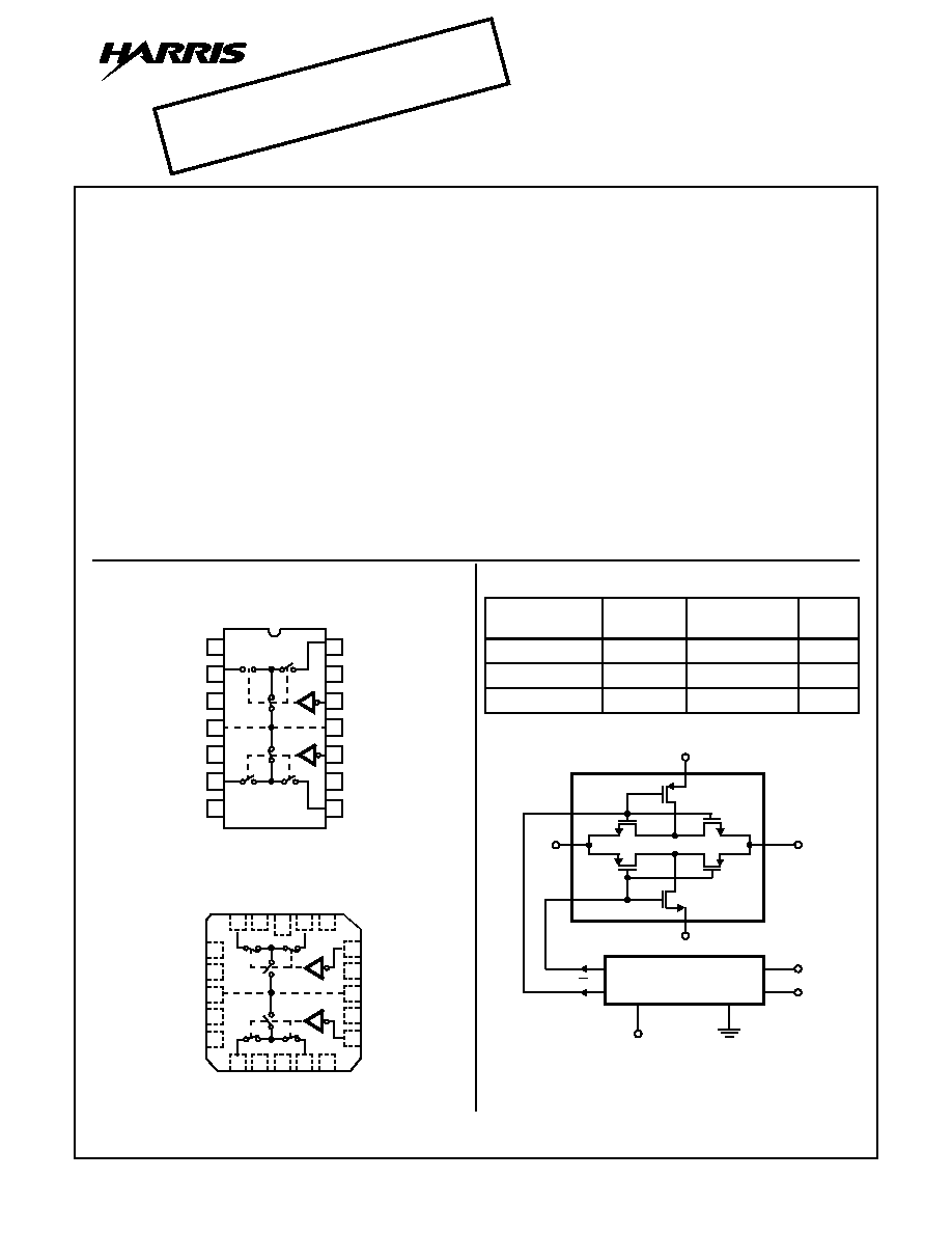
Pinouts
HI-222 (CERDIP, PDIP) (LOGIC "1" INPUT)
TOP VIEW
HI-222 (CLCC/PLCC) (LOGIC "0" INPUT)
TOP VIEW
Part Number Information
Functional Diagram
NOTE:
Source and Drain are arbitrarily depicted as Analog Input and Output, respectively. They may be interchanged without affecting
performance. All nonconnected pins should be tied to ground.
1
2
3
4
5
6
7
14
13
12
11
10
9
8
NC
GND
V+
NC
NC
V
IN2
V
IN1
NC
V-
NC
V
A1
V
OUT1
V
OUT2
V
A2
4
5
6
7
8
9
10
11
12
13
3
2
1
20 19
15
14
18
17
16
NC
V-
NC
GND
NC
V+
NC
NC
V
OUT1
V
IN1
V
OUT2
V
IN2
V
A2
V
A1
NC
NC
NC
NC
NC
NC
PART NUMBER
TEMP.
RANGE (
o
C)
PACKAGE
PKG.
NO.
HI4P0222-5
0 to 75
20 Ld PLCC
N20.35
HI1-0222-5
0 to 75
14 Ld CERDIP
F14.3
HI3-0222-5
0 to 75
14 Ld PDIP
E14.3
LOGIC INPUT
Q
LEVEL SHIFTER AND
DRIVER
V-
V+
V-
V+
IN
OUT
Q
CAUTION: These devices are sensitive to electrostatic discharge. Users should follow proper IC Handling Procedures.
Copyright
©
Harris Corporation 1997
File Number
3124.2
[ /Title
(HI-
222)
/Sub-
ject
(High
Fre-
quency/
Video
Switch)
/Author
()
/Key-
words
OBSOLETE PR
ODUCT
POSSIBLE SUBSTITUTE PR
ODUCT
HI-222/883
2
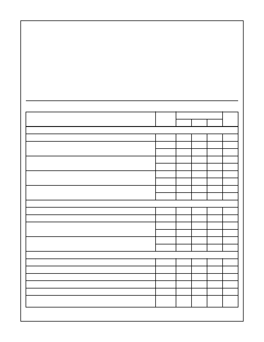
Absolute Maximum Ratings
T
A
= 25
o
C
Thermal Information
Supply Voltage (V+ to V-) (Terminals). . . . . . . . . . . . . . . . . . . . . 36V
±
V
S
to Ground (V+ to V-) . . . . . . . . . . . . . . . . . . . . . . . . . . . . .
±
18V
Digital Analog Input Voltage (V
A
, V
S
, V
D
) . . . . . . . . . . . . .
±
V
S
±
2V
I
PEAK
(S to D) (Pulse at 0.8ms, 10% Duty Cycle Max) . . . . . 100mA
I
PEAK
(Any Pin, 50% Duty Cycle). . . . . . . . . . . . . . . . . . . . . . . 28mA
Continuous Current (Any Pin). . . . . . . . . . . . . . . . . . . . . . . . . . 15mA
ESD Rating . . . . . . . . . . . . . . . . . . . . . . . . . . . . . . . . . . . . . <2000V
Operating Conditions
Temperature Range, HI-222-5 . . . . . . . . . . . . . . . . . . . .0
o
C to 75
o
C
Thermal Resistance (Typical, Note 1)
JA
(
o
C/W)
JC
(
o
C/W)
CERDIP Package . . . . . . . . . . . . . . . .
80
30
CLCC Package . . . . . . . . . . . . . . . . . .
70
18
PDIP Package . . . . . . . . . . . . . . . . . . .
90
N/A
PLCC Package . . . . . . . . . . . . . . . . . .
75
N/A
Maximum Junction Temperature (Hermetic Package) . . . . . . . . 175
o
C
Maximum Junction Temperature (Plastic Package) . . . . . . . . 150
o
C
Maximum Storage Temperature Range . . . . . . . . . .-65
o
C to 150
o
C
Maximum Lead Temperature (Soldering 10s) . . . . . . . . . . . . . 300
o
C
(PLCC - Lead Tips Only)
CAUTION: Stresses above those listed in "Absolute Maximum Ratings" may cause permanent damage to the device. This is a stress only rating and operation
of the device at these or any other conditions above those indicated in the operational sections of this specification is not implied.
NOTE:
1.
JA
is measured with the component mounted on an evaluation PC board in free air.
Electrical Specifications
±
V
S
=
±
15V, V
AH
= 2.0V, V
AL
= 0.8V, Unless Otherwise Specified
PARAMETER
TEMP (
o
C)
HI-222-5
UNITS
MIN
TYP
MAX
ANALOG SWITCH CHARACTERISTICS
V
S
, Analog Signal Range
Full
-15
-
+15
V
r
ON
, ON Resistance (Note 2)
25
-
35
50
Full
-
-
75
I
SOFF
Leakage
25
-
0.1
2.5
nA
Full
-
-
200
nA
I
DOFF
Leakage
25
-
0.1
2.5
nA
Full
-
-
200
nA
I
DON
Leakage
25
-
0.3
2.5
A
Full
-
-
200
nA
DIGITAL INPUT CHARACTERISTICS
V
AL
, Low Threshold
Full
-
-
0.8
V
V
AH
, High Threshold
Full
2.0
-
-
V
I
AL
, Low Level Leakage
25
-
0.1
1.0
µ
A
Full
-
-
1.0
µ
A
I
AH
, High Level Leakage
25
-
0.1
1.0
µ
A
Full
-
-
1.0
µ
A
SWITCHING CHARACTERISTICS
t
ON
(Note 3)
25
-
100
200
ns
t
OFF
(Note 3)
25
-
70
200
ns
Off-Isolation at 10MHz (Note 4)
25
-
-65
-
dB
Crosstalk at 10MHz (Note 4)
25
-
-80
-
dB
Differential Gain (Note 5)
25
-
0.03
-
%
Differential Phase (Note 5)
25
-
0.003
-
De-
grees
HI-222
3
Gain Tolerance At 1MHz (Note 6)
At 8MHz
25
-
0.05
-
dB
25
-
0.15
-
dB
Bandwidth (Note 6)
25
-
200
-
MHz
C
S(OFF)
, Switch Input Capacitance
25
-
12
-
pF
C
D(OFF)
, Switch Output Capacitance
25
-
28
-
pF
C
D(ON)
, Switch Output Capacitance
25
-
83
-
pF
C
A(ON)
, Switch Output Capacitance
25
-
5
-
pF
C
DS(OFF)
, Drain-to-Source Capacitance
25
-
0.2
-
pF
POWER REQUIREMENTS
1
±
at
±
15V Quiescent Current
25
-
2.5
4.0
mA
Full
-
-
6.0
mA
P
D
, Quiescent Power Dissipation
25
-
75
120
mW
Full
-
-
180
mW
NOTES:
2. As with all semiconductors, stresses listed under "Absolute Maximum Ratings" may be applied to devices (one at a time) without resulting
in permanent damage. This is a stress rating only. Exposure to absolute maximum rating conditions for extended periods may affect
device reliability. The conditions listed under "Electrical Specifications" are the only conditions recommended for satisfactory operation.
3. V
OUT
=
±
5V, I
OUT
- 7.5mA.
4. V
IN
= +5V, R
L
= 2k
, C
L
= 40pF. V
A
levels are 0.0V to 3.0V for switch under test. Switch not under test has V
A
= 4.0V.
5. V
IN
= 300mV
P-P
, R
L
= 50
, V
AH
= +2.0V, V
AL
= 0.8, f = 10MHz.
6. V
IN
= 300mV
P-P
, V
OFFSET
= 1.0, f = 3.58MHz and 4.43MHz, V
AL
= 0.V, R
L
= 2k
.
7. V
IN
= 300mV
P-P
R
L
= 50
, V
AL
= 0.8V.
Test Circuits
FIGURE 1. SWITCHING TEST CIRCUIT (t
ON
, t
OFF1
)
Electrical Specifications
±
V
S
=
±
15V, V
AH
= 2.0V, V
AL
= 0.8V, Unless Otherwise Specified (Continued)
PARAMETER
TEMP (
o
C)
HI-222-5
UNITS
MIN
TYP
MAX
V+ = +15V
SWITCH INPUT
V
IN
= +5
LOGIC
INPUT
2
GND
V
A
12
4
14
3
11
V- = -15V
R
L
2K
C
L
35pF
V
OUT
V
O
= V
IN
R
L
R
L
+ r
ON
-------------------------
C
L
Includes C
FIXTURE
+ C
PROBE
HI-222
4
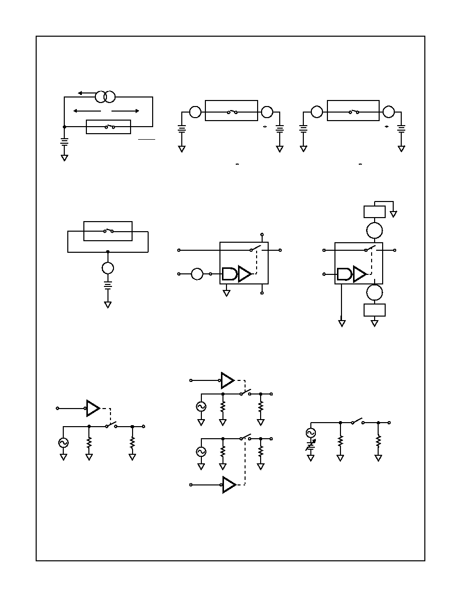
Test Circuits
(Continued)
R
DS
7.5mA
V
2
IN
OUT
±
5V
r
ON
=
V
2
7.5mA
V
IN
=
±
5V, I = 7.5mA, V
A
= 0.8V
OUT
IN
A
A
I
S
(OFF)
I
D
(OFF)
±
5V
+5V
I
S
(OFF)
V
IN
=
±
5V, V
OUT
= +5V, V
A
= 2.0V
I
D
(OFF)
OUT
IN
A
A
I
S
(OFF)
I
D
(OFF)
±
5V
+5V
V
IN
=
±
5V, V
OUT
= +5V, V
A
= 2.0V
A
I
D(ON)
IN
OUT
I
D(ON)
±
5V
V
IN
=
±
5V, V
OUT
=
±
5V V
A
= 0.8V
IN
V
A
+V
CC
-V
CC
GND
OUT
ADDRESS CURRENT
V
AH
= 2.0V, V
AL
= 0.8V
I
A
GND
OUT
IN
-V
CC
-I
CC
+I
CC
+V
CC
V
A
SUPPLY CURRENTS
V
A
= 0.8V, 2.0V
OFF ISOLATION
V
IN
= 300mV
P-P
, f = 10MHz. R
IN
= R
L
= 50
,
V
A1
= 2.0V
V
A1
V
IN
R
IN
R
L
V
OUT
CROSSTALK
V
A1
V
IN
R
IN
R
L
R
IN
R
L
V
IN
V
A2
V
IN
= 300mV
P-P
, f = 10MHz R
IN
= R
L
= 50
,
V
A1
= 2.0V, V
A2
= 0.8V
DIFFERENTIAL GAIN, PHASE
V
IN
V
DC
V
AC
R
IN
R
L
V
OUT
V
AC
= 300mV
P-P
, f = 3.58MHz AND 4.43MHz,
V
DC
= 0.0V TO 1.0V, R
L
= 2k
, R
IN
= 50
HI-222
5
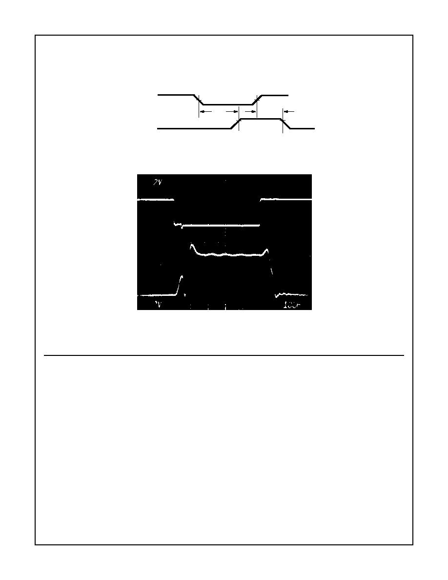
Switching Waveforms
FIGURE 2. LOGIC "0" = SWITCH ON
FIGURE 3. t
ON
, t
OFF
, V
AL
= 0.0V, V
AH
= 3.0V
DIGITAL
INPUT
SWITCH
OUTPUT
V
AH
= 3.0V
50%
V
AL
= 0.0V
50%
t
ON
t
OFF1
90%
0V
90%
LOGIC "0" = SWITCH ON
TOP: (2V/DIV.)
BOTTOM: OUTPUT (2V/DIV.)
HORIZONTAL: 100ns/DIV.
HI-222