1
File Number
3148.2
HI-524
4-Channel Wideband and Video
Multiplexer
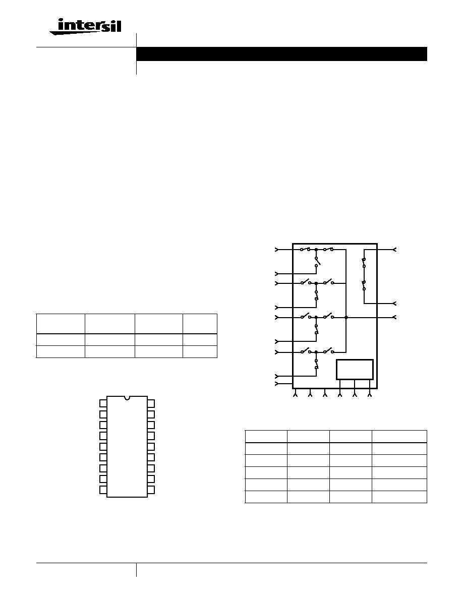
The HI-524 is a 4-Channel CMOS analog multiplexer designed
to process single-ended signals with bandwidths up to 10MHz.
The chip includes a 1 of 4 decoder for channel selection and an
enable input to inhibit all channels (chip select).
Three CMOS transmission gates are used in each channel,
as compared to the single gate in more conventional CMOS
multiplexers. This provides a double barrier to the unwanted
coupling of signals from each input to the output. In addition,
Dielectric Isolation (DI) processing helps to insure the
Crosstalk is less than -60dB at 10MHz.
The HI-524 is designed to operate into a wideband buffer
amplifier such as the Intersil HA-2541. The multiplexer chip
includes two "ON" switches in series, for use as a feedback
element with the amplifier. This feedback resistance
matches and tracks the channel ON resistance, to minimize
the amplifier V
OS
and its variation with temperature.
The HI-524 is well suited to the rapid switching of video and
other wideband signals in telemetry, instrumentation, radar
and video systems.
Pinout
HI-524 (CERDIP, PDIP)
TOP VIEW
Features
∑ Crosstalk (10MHz) . . . . . . . . . . . . . . . . . . . . . . . . < -60dB
∑ Fast Access Time . . . . . . . . . . . . . . . . . . . . . . . . . 150ns
∑ Fast Settling Time . . . . . . . . . . . . . . . . . . . . . . . . . 200ns
∑ TTL Compatible
Applications
∑ Wideband Switching
∑ Radar
∑ TV Video
∑ ECM
Functional Diagram
Ordering Information
PART
NUMBER
TEMP. RANGE
(
o
C)
PACKAGE
PKG. NO.
HI1-0524-5
0 to 75
18 Ld CERDIP
F18.3
HI3-0524-5
0 to 75
18 Ld PDIP
E18.3
10
11
12
13
14
15
16
17
18
9
8
7
6
5
4
3
2
1
FB (IN)
FB (OUT)
SIG GND
IN2
SIG GND
IN1
EN
-V
A
0
+V
OUT
SIG GND
SIG GND
IN4
SIG GND
SUPPLY GND
IN3
A
1
TRUTH TABLE
A
1
A
0
EN
ON CHANNEL
X
X
L
None
L
L
H
1 (Note)
L
H
H
2
H
L
H
3
H
H
H
4
NOTE: Channel 1 is shown selected in the Functional Diagram.
1 OF 4
DECODER
FB (IN)
FB (OUT)
OUTPUT
IN1
SIG GND
SIG GND
IN2
IN3
SIG GND
IN4
SIG GND
SIG GND
-15V SUP
GND
+15V
EN
A
0
A
1
1
Data Sheet
July 1999
CAUTION: These devices are sensitive to electrostatic discharge; follow proper IC Handling Procedures.
1-888-INTERSIL or 321-724-7143
|
Copyright
©
Intersil Corporation 1999
2
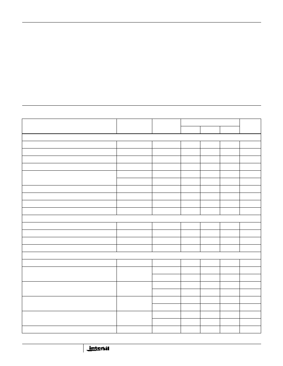
Absolute Maximum Ratings
Thermal Information
V+ to V- . . . . . . . . . . . . . . . . . . . . . . . . . . . . . . . . . . . . . . . . . . . 33V
Digital Input Voltage (V
EN
, V
A
) . . . . . . . . . . . . . . . . . . . . -6V to +6V
Analog Signal (V
IN
, V
OUT
). . . . . . . . . . . . . . . . . (V-) -2V to (V+) +2V
Either Supply to Ground. . . . . . . . . . . . . . . . . . . . . . . . . . . . . . 16.5V
Operating Conditions
Temperature Range
HI-524-5 . . . . . . . . . . . . . . . . . . . . . . . . . . . . . . . . . . 0
o
C to 75
o
C
Thermal Resistance (Typical, Note 1)
JA
(
o
C/W)
JC
(
o
C/W)
CERDIP Package . . . . . . . . . . . . . . . . .
75
20
PDIP Package . . . . . . . . . . . . . . . . . . .
80
N/A
Maximum Junction Temperature
Ceramic Package . . . . . . . . . . . . . . . . . . . . . . . . . . . . . . . . 175
o
C
Plastic Package . . . . . . . . . . . . . . . . . . . . . . . . . . . . . . . . . 150
o
C
Maximum Storage Temperature. . . . . . . . . . . . . . . . -65
o
C to 150
o
C
Maximum Lead Temperature (Soldering, 10s). . . . . . . . . . . . 300
o
C
CAUTION: Stresses above those listed in "Absolute Maximum Ratings" may cause permanent damage to the device. This is a stress only rating and operation of the
device at these or any other conditions above those indicated in the operational sections of this specification is not implied.
NOTE:
1.
JA
is measured with the component mounted on an evaluation PC board in free air.
Electrical Specifications
Supplies = +15V, -15V; V
AH
(Logic Level High) = 2.4V, V
AL
(Logic Level Low) = 0.5V; V
EN
= 2.4V,
Unless Otherwise Specified
PARAMETER
TEST
CONDITIONS
TEMP
(
o
C)
-5
UNITS
MIN
TYP
MAX
DYNAMIC CHARACTERISTICS
Access Time, t
A
Note 5
25
-
150
300
ns
Break-Before-Make Delay, t
OPEN
Note 5
25
-
20
-
ns
Enable Delay (ON), t
ON (EN)
R
L
= 500
25
-
180
-
ns
Enable Delay (OFF), t
OFF (EN)
R
L
= 500
25
-
180
-
ns
Settling Time (Note 5)
To 0.1%
25
-
200
-
ns
To 0.01%
25
-
600
-
ns
Crosstalk
Note 6
25
-
-65
-
dB
Channel Input Capacitance, C
S(OFF)
25
-
4
-
pF
Channel Output Capacitance, C
D(OFF)
25
-
10
-
pF
Digital Input Capacitance, C
A
25
-
5
-
pF
DIGITAL INPUT SPECIFICATIONS
Input Low Threshold (TTL), V
AL
Full
-
-
0.8
V
Input High Threshold (TTL), V
AH
Full
2.4
-
-
V
Input Leakage Current (High), I
AH
Full
-
0.05
1
µ
A
Input Leakage Current (Low), I
AL
Full
-
-
25
µ
A
ANALOG CHANNEL SPECIFICATIONS
Analog Signal Range, V
lN
Full
-10
-
+10
V
On Resistance, r
ON
Note 2
25
-
700
-
Full
-
-
1.5
k
Off Input Leakage Current, I
S (OFF)
Note 3
25
-
0.2
-
nA
Full
-
-
50
nA
Off Output Leakage Current, I
D (OFF)
Note 3
25
-
0.2
-
nA
Full
-
-
50
nA
On Channel Leakage Current, I
D (ON)
Note 3
25
-
0.7
-
nA
Full
-
-
50
nA
-3dB Bandwidth
Note 4
25
-
8
-
MHz
HI-524
3
POWER SUPPLY CHARACTERISTICS
Power Dissipation, P
D
Full
-
-
750
mW
Current, I+
Note 7
Full
-
-
25
mA
Current, I-
Note 7
Full
-
-
25
mA
NOTES:
2. V
lN
= 0V; l
OUT
= 100
µ
A (See Test Circuit section).
3. V
O
=
±
10V; V
IN
=
±
10V. (See Test Circuit section).
4. MUX output is buffered with HA-5033 amplifier.
5. 6V Step,
±
3V to
3V, See Test Circuit section.
6. V
IN
= 10MHz, 3V
P-P
on one channel, with any other channel selected. (Worst case is channel 3 selected with input on channel 4.) MUX output
is buffered with HA-2541 as shown in Applications section. Terminate all channels with 75
.
7. Supply currents vary less than 0.5mA for switching rates from DC to 2MHz.
Electrical Specifications
Supplies = +15V, -15V; V
AH
(Logic Level High) = 2.4V, V
AL
(Logic Level Low) = 0.5V; V
EN
= 2.4V,
Unless Otherwise Specified (Continued)
PARAMETER
TEST
CONDITIONS
TEMP
(
o
C)
-5
UNITS
MIN
TYP
MAX
±
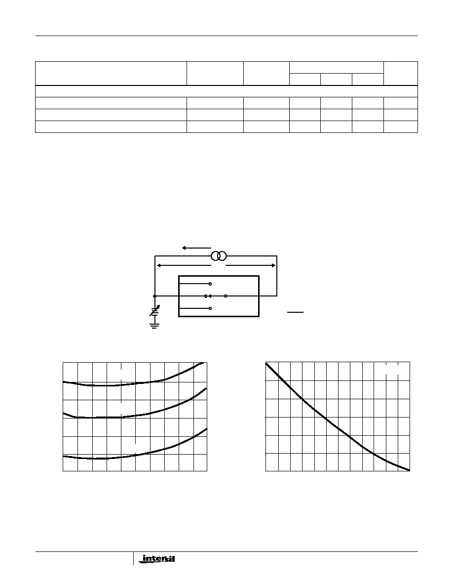
Test Circuits and Waveforms
T
A
= 25
o
C, V
SUPPLY
=
±
15V, V
AH
= 2.4V, V
AL
= 0.8V, Unless Otherwise Specified
FIGURE 1A. TEST CIRCUIT
FIGURE 1B. ON RESISTANCE vs ANALOG INPUT VOLTAGE
FIGURE 1C. ON RESISTANCE vs SUPPLY VOLTAGE
FIGURE 1. ON RESISTANCE
I
OUT
100
µ
A
OUT
IN
V
IN
r
ON
=
V
2
100
µ
A
V
2
25
o
C
125
o
C
-55
o
C
V
IN
(V)
-10
-8
-6
-4
-2
0
2
4
6
8
10
1,000
900
800
700
600
500
400
r
ON
(
)
1,000
900
800
700
9
10
11
12
13
14
15
SUPPLY VOLTAGE (
±
V)
r
ON
(
)
V
IN
= 0V
HI-524
4
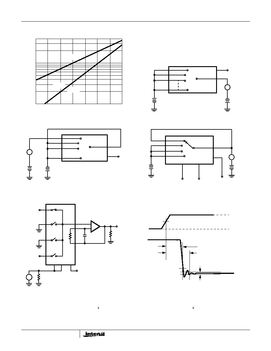
FIGURE 2A. LEAKAGE CURRENT vs TEMPERATURE
FIGURE 2B. I
D(OFF)
TEST CIRCUIT (NOTE 8)
FIGURE 2C. I
S(OFF)
TEST CIRCUIT (NOTE 8)
FIGURE 2D. I
D(ON)
TEST CIRCUIT (NOTE 8)
FIGURE 2. LEAKAGE CURRENTS
FIGURE 3A. TEST CIRCUIT
FIGURE 3B. MEASUREMENT POINTS
FIGURE 3. SETTLING TIME, ACCESS TIME, BREAK-BEFORE-MAKE DELAY (NOTE 9)
NOTES:
8. Two measurements per channel:
±
10V and 10V. (Two measurements per device for I
D(OFF)
±
10V and 10V.)
9. The Break-Before-Make test requires inputs 1 and 4 at the same voltage.
10. Capacitor value may be selected to optimize AC performance.
Test Circuits and Waveforms
T
A
= 25
o
C, V
SUPPLY
=
±
15V, V
AH
= 2.4V, V
AL
= 0.8V, Unless Otherwise Specified (Continued)
I
D(ON)
0
25
50
75
100
125
150
TEMPERATURE (
o
C)
1.0
0.1
LEAKA
GE CURRENT (nA)
I
S(OFF)
I
D(OFF)
OUT
I
D(OFF)
A
10V
±
±
10V
0.8V
EN
OUT
I
S(OFF)
10V
±
±
10V
0.8V
EN
A
OUT
I
D(ON)
A
10V
±
±
10V
+2.4V
EN
A
1
A
0
+
-
HA-2541
3V
2
18
16
20pF
OUTPUT
HA-524
5V
EN
A
1
A
0
±
±
3V
75
(NOTE 10)
IN1
IN2
IN3
IN4
V
A
50
ADDRESS DRIVE (V
A
)
1.6V
+3V
10%
-3V
V
AL
= 0.8V
V
AH
= 2.4V
ACCESS TIME, t
A
SETTLING TIME, t
S
HA-2541
OUTPUT
±
0.1% OF FULL SCALE
(OR
±
0.01%)
HI-524
5
Application Information
Often it is desirable to buffer the Hl-524 output, to avoid
loading errors due to the channel "ON" resistance:
The buffer amplifier should offer sufficient bandwidth and
slew rate to avoid degradation of the anticipated signals. For
video switching, the HA-5033 and HA-2542 offer good
performance plus
±
100mA output current for driving coaxial
cables. For general wideband applications, the HA-2541
offers the convenience of unity gain stability plus 90ns
settling (to
±
0.1%) and
±
10V output swing. Also, the Hl-524
includes a feedback resistance for use with the HA-2541.
This resistance matches and tracks the channel "ON"
resistance, to minimize offset voltage due to the buffer's bias
currents.
Note that the on-chip feedback element between pins 16 and
18 includes two switches in series, to simulate a channel
resistance. These switches open for V
EN
= Low. This allows
two or more Hl-524s to operate into one HA-2541, with their
feedback elements connected in parallel. Thus, only the
selected multiplexer provides feedback, and the amplifier
remains stable.
All Hl-524 pins labeled `SlG GND' (pins 3, 4, 6, 13, 15)
should be externally connected to signal ground for best
crosstalk performance.
Bypass capacitors (0.1
µ
F to 1
µ
F) are recommended from
each HI-524 supply pin to power ground (pins 1 and 17 to
pin 8). Locate the buffer amplifier near the Hl-524 so the two
capacitors may bypass both devices.
If an analog input 1V or greater is present when supplies are
off, a low resistance is seen from that input to a supply line.
(For example, the resistance is approximately 160
for an
input of -3V.) Current flow may be blocked by a diode in each
supply line, or limited by a resistor in series with each
channel. The best solution, of course, is to arrange that no
digital or analog inputs are present when the power supplies
are off.
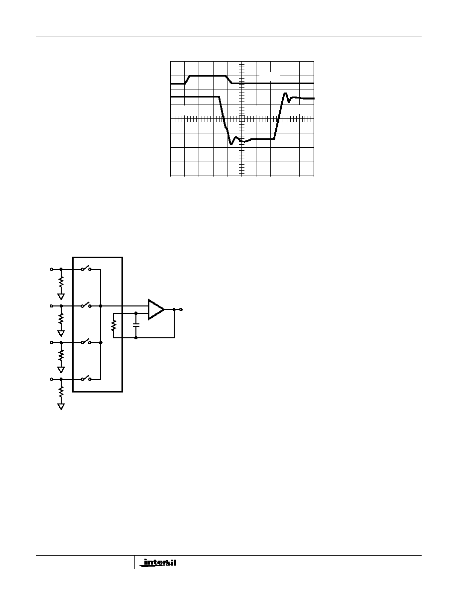
FIGURE 4. ACCESS TIME WAVEFORMS
Test Circuits and Waveforms
T
A
= 25
o
C, V
SUPPLY
=
±
15V, V
AH
= 2.4V, V
AL
= 0.8V, Unless Otherwise Specified (Continued)
50ns/DIV.
1V/DIV.
5V/DIV.
S
4
ON
S
1
ON
V
A
INPUT
OUTPUT
+
-
HA-2541
14
BUFFERED
CH2
75
7
CH3
75
5
75
CH4
12
CH1
75
2
18
16
20pF (NOTE)
OUTPUT
HA-524
NOTE: Capacitor value may be selected to optimize AC performance.
FIGURE 5.
HI-524