 | ÐлекÑÑоннÑй компоненÑ: HI3306/10 | СкаÑаÑÑ:  PDF PDF  ZIP ZIP |
HI3306
1
December 1997
HI3306
6-Bit, 15 MSPS, Flash A/D Converter
Features
· CMOS Low Power (Typ). . . . . . . . . . . . . . . . . . . . .55mW
· Parallel Conversion Technique
· Single Power Supply Voltage . . . . . . . . . . . . 3V to 7.5V
· Sampling Rate with Single 5V Supply . . . . . . . . 15MHz
· 6-Bit Latched Three-State Output with Overflow Bit
· Linearity (INL, DNL):
- HI3306JIP/15 . . . . . . . . . . . . . . . . . . . . . . . . .
±
0.5 LSB
- HI3306JIP/10 . . . . . . . . . . . . . . . . . . . . . . . . .
±
0.5 LSB
- HI3306JIB/15 . . . . . . . . . . . . . . . . . . . . . . . . .
±
0.5 LSB
- HI3306JIB/10 . . . . . . . . . . . . . . . . . . . . . . . . .
±
0.5 LSB
· Sampling Rate:
- HI3306JIP/15 . . . . . . . . . . . . . . . . . . . . . 15MHz (67ns)
- HI3306JIP/10 . . . . . . . . . . . . . . . . . . . . 10MHz (100ns)
- HI3306JIB/15 . . . . . . . . . . . . . . . . . . . . . 15MHz (67ns)
- HI3306JIB/10 . . . . . . . . . . . . . . . . . . . . 10MHz (100ns)
Applications
· Video Digitizing
· Digital Communication Systems
· High Speed Data Acquisition
· Radar Signal Processing
Description
The HI3306 family are CMOS parallel (FLASH) analog-to-
digital converters designed for applications demanding
both low power consumption and high speed digitization.
Digitizing at 15MHz, for example, requires only about
55mW.
The HI3306 family operates over a wide, full scale signal input
voltage range of 1V up to the supply voltage. Power consump-
tion is as low as 15mW, depending upon the clock frequency
selected. The HI3306 offers improved linearity at a lower ref-
erence voltage and high operating speed with a 5V supply.
The overflow bit makes possible the connection of two or
more HI3306s in series to increase the resolution of the
conversion system.
Sixty-four paralleled auto balanced comparators measure
the input voltage with respect to a known reference to pro-
duce the parallel bit outputs in the HI3306. Sixty-three com-
parators are required to quantize all input voltage levels in
this 6-bit converter, and the additional comparator is
required for the overflow bit.
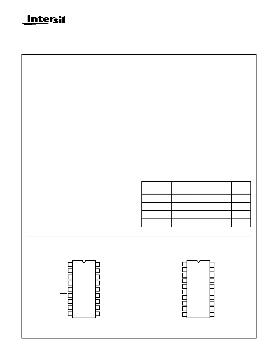
Pinouts
Ordering Information
PART NUMBER
TEMP.
RANGE (
o
C)
PACKAGE
PKG. NO.
HI3306JIP/15
-40 to 85
18 Ld PDIP
E18.3
HI3306JIP/10
-40 to 85
18 Ld PDIP
E18.3
HI3306JIB/15
-40 to 85
20 Ld SOIC
M20.3
HI3306JIB/10
-40 to 85
20 Ld SOIC
M20.3
HI3306 (PDIP)
TOP VIEW
HI3306 (SOIC)
TOP VIEW
10
11
12
13
14
15
16
17
18
9
8
7
6
5
4
3
2
1
(MSB) B6
OVERFLOW
V
SS
V
Z
CE2
CLK
CE2
PHASE
V
REF
+
B5
REF
B3
B2
B4
B1 (LSB)
V
DD
V
IN
V
REF
-
CENTER
11
12
13
14
15
16
17
18
20
19
10
9
8
7
6
5
4
3
2
1
(MSB) B6
OVERFLOW
V
SS
NC
V
Z
CE2
CLK
CE1
PHASE
V
REF
+
B5
REF
B3
B2
B4
B1 (LSB)
V
DD
NC
V
IN
V
REF
-
CENTER
File Number
4136.2
CAUTION: These devices are sensitive to electrostatic discharge; follow proper IC Handling Procedures.
1-888-INTERSIL or 321-724-7143 | Copyright © Intersil Corporation 1999
2
Functional Block Diagram
Typical Application Circuit
ENCODER
LOGIC
COMP
1
V
SS
1 (AUTO BALANCE)
2 (SAMPLE UNKNOWN)
50k
CLOCK
V
REF
-
V
REF
+
V
IN
V
DD
1
1
1
2
2
R
R/2
R
R
R
THREE-STATE
R/2
D Q
CL
D Q
CL
D Q
CL
D Q
CL
D Q
CL
D Q
CL
D Q
CL
AND
LATCHES
COMPARATOR
COMP
2
COMP
32
COMP
63
COMP
64
REF
CENTER
120
R
R
PHASE
ZENER
DIODE
V
SS
6.2V NOMINAL
OVERFLOW
CE1
CE2
B6 (MSB)
B5
B4
B3
B2
B1 (LSB)
B6
OF
V
SS
V
Z
CE2
CLK
CE1
PH
V
REF+
B5
RC
B3
B2
B4
B1
V
DD
V
IN
V
REF-
HI3306
CLOCK
CA741CE
+12V
560
5k
+5V
6.2V
+12V
0.1
µ
F
+
-
0.2
µ
F
10
µ
F
+5V
SIGNAL
INPUT
DATA
OUTPUT
OF
B6
B5
B4
B3
B2
B1
(LSB)
0.1
µ
F
10
11
12
13
14
15
16
17
18
9
8
7
6
5
4
3
2
1
HI3306
HI3306
3
HI3306
Absolute Maximum Ratings
Thermal Information
DC Supply Voltage Range, V
DD
Voltage Referenced to V
SS
Terminal . . . . . . . . . . . -0.5V to +8.5V
Input Voltage Range
All Inputs Except Zener. . . . . . . . . . . . . . . . . -0.5V to V
DD
+ 0.5V
DC Input Current
CLK, PH, CE1, CE2, V
IN
. . . . . . . . . . . . . . . . . . . . . . . . .
±
20mA
Operating Conditions
Supply Voltage Range . . . . . . . . . . . . . . . . . . . . . . . . . . . . .3V to 8V
Temperature Range (T
A
) . . . . . . . . . . . . . . . . . . . . . . -40
o
C to 85
o
C
Thermal Resistance (Typical, Note 1)
JA
(
o
C/W)
PDIP Package . . . . . . . . . . . . . . . . . . . . . . . . . . . . .
75
SOIC Package . . . . . . . . . . . . . . . . . . . . . . . . . . . . .
100
Maximum Junction Temperature . . . . . . . . . . . . . . . . . . . . . . . 150
o
C
Maximum Storage Temperature Range . . . . . . . . . .-65
o
C to 150
o
C
Maximum Lead Temperature (Soldering 10s) . . . . . . . . . . . . . 300
o
C
(SOIC - Lead Tips Only)
CAUTION: Stresses above those listed in "Absolute Maximum Ratings" may cause permanent damage to the device. This is a stress only rating and operation
of the device at these or any other conditions above those indicated in the operational sections of this specification is not implied.
NOTE:
1.
JA
is measured with the component mounted on an evaluation PC board in free air.
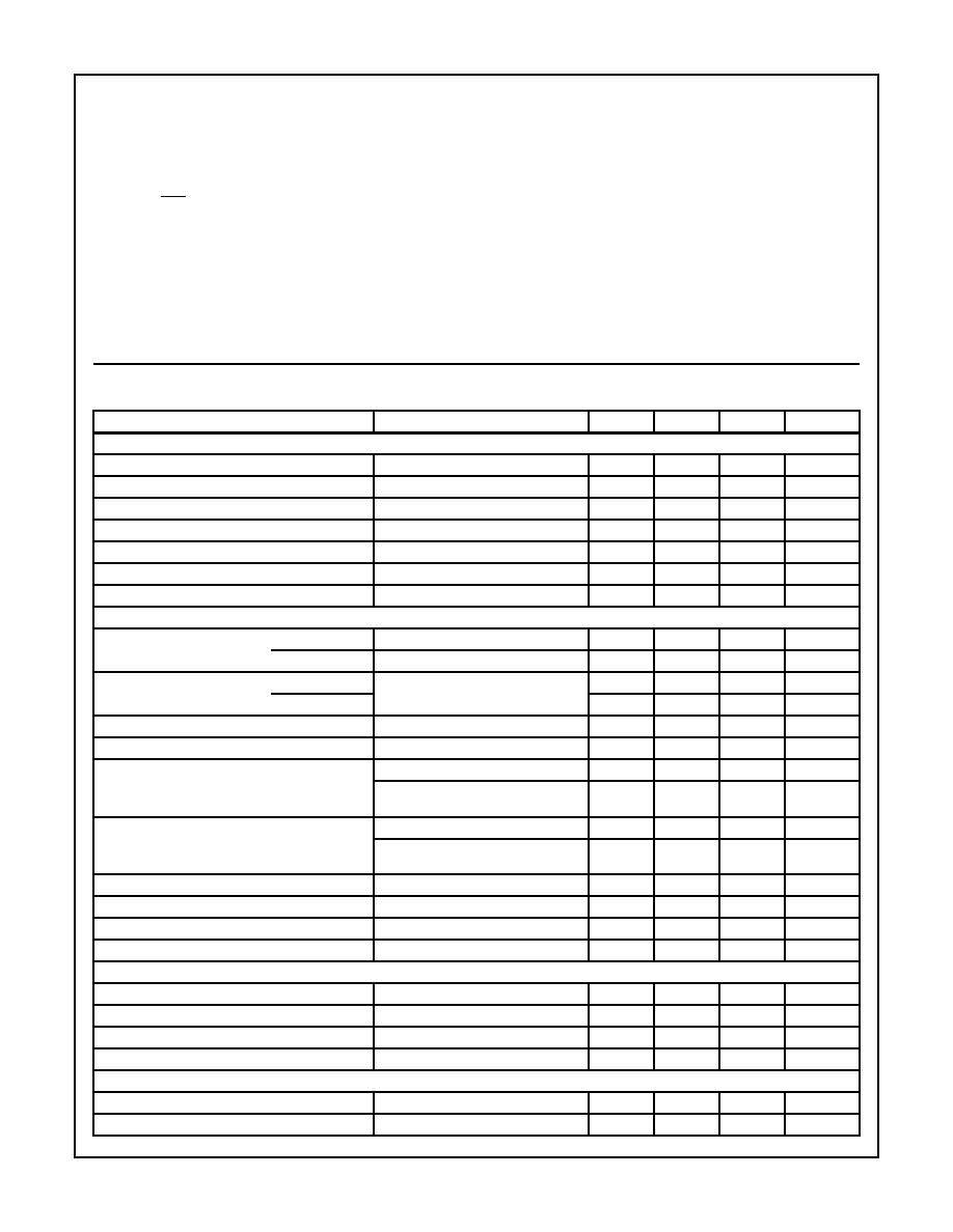
Electrical Specifications
T
A
= 25
o
C, V
DD
= 5V, V
REF
+ = 4.8V, V
SS
= V
REF
- = GND, Clock = 15MHz Square Wave for
HI3306XXX/15, 10MHz for HI3306XXX/10
PARAMETER
TEST CONDITIONS
MIN
TYP
MAX
UNITS
SYSTEM PERFORMANCE
Resolution
6
-
-
Bits
Integral Linearity Error, INL
-
±
0.25
±
0.5
LSB
Differential Linearity Error, DNL
-
±
0.25
±
0.5
LSB
Offset Error (Unadjusted)
(Note 2)
-
±
0.5
±
1
LSB
Gain Error (Unadjusted)
(Note 3)
-
±
0.5
±
1
LSB
Gain Temperature Coefficient
-
+0.1
-
mV/
o
C
Offset Temperature Coefficient
-
-0.1
-
mV/
o
C
DYNAMIC CHARACTERISTICS Input Signal Level 0.5dB Below Full Scale
Maximum Conversion Speed
HI3306XXX/10
10
13
-
MSPS
HI3306XXX/15
15
20
-
MSPS
Maximum Conversion Speed
HI3306XXX/10
(Note 5)
1,
2
Minimum
12
-
-
MSPS
HI3306XXX/15
18
-
-
MSPS
Allowable Input Bandwidth
(Note 5)
DC
-
f
CLOCK/2
MHz
-3dB Input Bandwidth
-
30
-
MHz
Signal to Noise Ratio, SNR
f
S
= 15MHz, f
IN
= 100kHz
-
34.6
-
dB
f
S
= 15MHz, f
IN
= 5MHz
-
33.4
-
dB
Signal to Noise Ratio, SINAD
f
S
= 15MHz, f
IN
= 100kHz
-
34.2
-
dB
f
S
= 15MHz, f
IN
= 5MHz
-
29.0
-
dB
Total Harmonic Distortion, THD
f
S
= 15MHz, f
IN
= 100kHz
-
-46.0
-
dBc
f
S
= 15MHz, f
IN
= 5MHz
-
-30.0
-
dBc
Effective Number of Bits, ENOB
f
S
= 15MHz, f
IN
= 100kHz
-
5.5
-
Bits
f
S
= 15MHz, f
IN
= 5MHz
-
4.5
-
Bits
ANALOG INPUTS
Positive Full Scale Input Range
(Notes 4, 5)
1
4, 8
V
DD
+ 0.5
V
Negative Full Scale Input Range
(Notes 4, 5)
-0.5
0
V
DD
- 1
V
Input Capacitance
-
15
-
pF
Input Current
V
IN
= 4.92V, V
DD
= 5V
-
-
±
500
µ
A
INTERNAL VOLTAGE REFERENCE
Zener Voltage
I
Z
= 10mA
5.4
6.2
7.4
V
Zener Dynamic Impedance
I
Z
= 10mA, 20mA
-
12
25
=
RMS Signal
RMS Noise
----------------------------------
=
RMS Signal
RMS Noise + Distortion
------------------------------------------------------------------
4
Zener Temperature Coefficient
-
-0.5
-
mV/
o
C
REFERENCE INPUTS
Resistor Ladder Impedance
650
1100
1550
DIGITAL INPUTS
Maximum V
IN
, Logic 0
All Digital Inputs (Note 5)
-
-
0.3 x V
DD
V
Maximum V
IN
, Logic 1
All Digital Inputs (Note 5)
0.7 x V
DD
-
-
V
Digital Input Current
Except CLK, V
IN
= 0V, 5V
-
±
1
±
5
µ
A
Digital Input Current
CLK Only
-
±
100
±
200
µ
A
DIGITAL OUTPUTS
Digital Output Three-State Leakage
V
OUT
= 0V, 5V
-
±
1
±
5
µ
A
Digital Output Source Current
V
OUT
= 4.6V
-1.6
-
-
mA
Digital Output Sink Current
V
OUT
= 0.4V
3.2
-
-
mA
TIMING CHARACTERISTICS
Auto Balance Time (
1)
HI3306XXX/10
50
-
ns
HI3306XXX/15
33
-
Sample Time (
2)
HI3306XXX/10
(Note 5)
33
-
5000
ns
HI3306XXX/15
22
-
5000
ns
Aperture Delay
-
8
-
ns
Aperture Jitter
-
100
-
ps
P-P
Output Data Valid Delay, t
D
HI3306XXX/10
-
35
50
ns
HI3306XXX/15
-
30
40
ns
Output Data Hold Time, t
H
(Note 5)
15
25
-
ns
Output Enable Time, t
EN
-
20
-
ns
Output Disable Time, t
DIS
-
15
-
ns
POWER SUPPLY CHARACTERISTICS
I
DD
Current, Refer to Figure 4 HI3306XXX/10
Continuous Conversion (Note 5)
-
11
20
mA
HI3306XXX/15
-
14
25
mA
I
DD
Current
Continuous
1
-
7.5
15
mA
NOTES:
2. OFFSET ERROR is the difference between the input voltage that causes the 00 to 01 output code transition and (V
REF
+ - V
REF
-)/128.
3. GAIN ERROR is the difference the input voltage that causes the 3F
16
to overflow output code transition and (V
REF
+ - V
REF
-) x 127/128.
4. The total input voltage range, set by V
REF
+ and V
REF
-, may be in the range of 1 to (V
DD
+ 1) V.
5. Parameter not tested, but guaranteed by design or characterization.
Electrical Specifications
T
A
= 25
o
C, V
DD
= 5V, V
REF
+ = 4.8V, V
SS
= V
REF
- = GND, Clock = 15MHz Square Wave for
HI3306XXX/15, 10MHz for HI3306XXX/10 (Continued)
PARAMETER
TEST CONDITIONS
MIN
TYP
MAX
UNITS
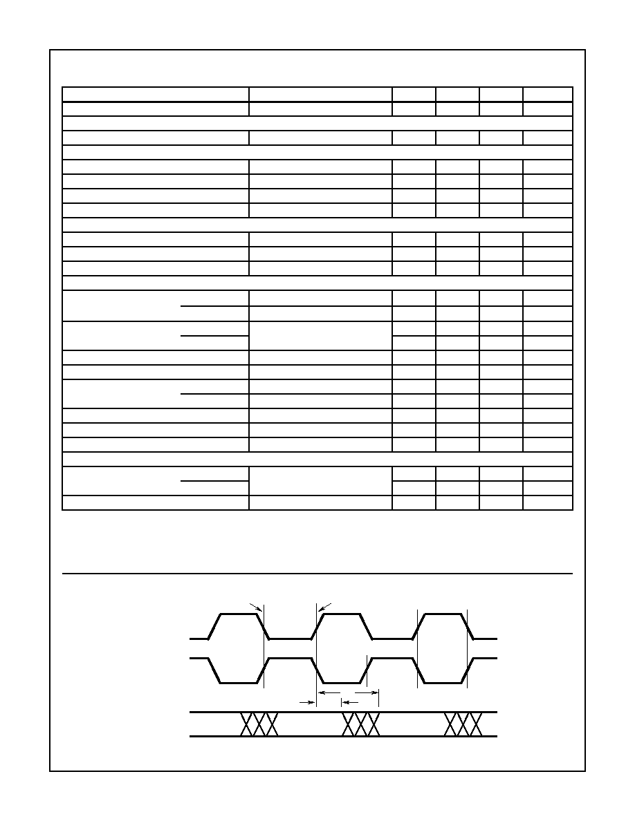
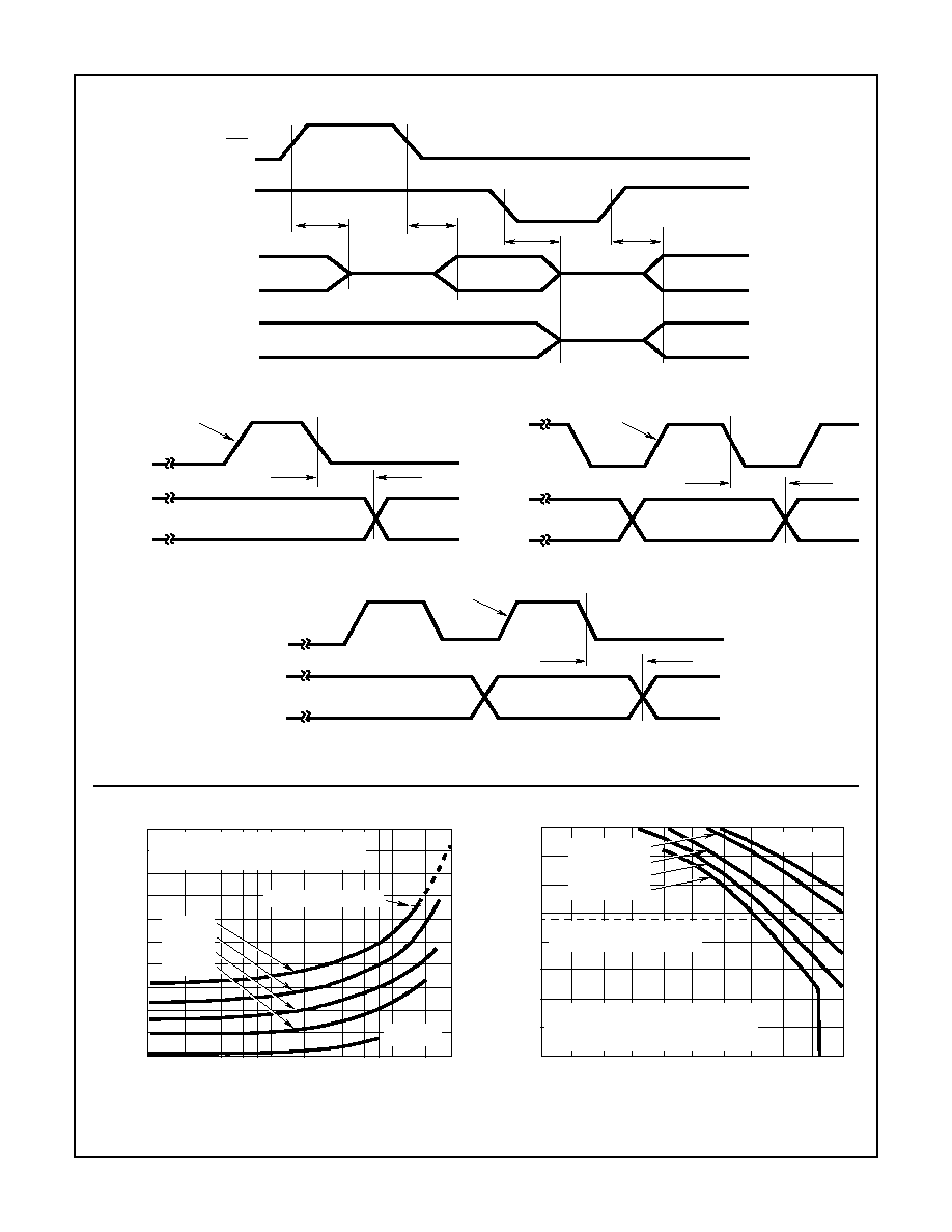
Timing Waveforms
FIGURE 1. INPUT-TO-OUTPUT
CLOCK IF
PHASE IS HIGH
CLOCK IF
PHASE IS LOW
COMPARATOR DATA IS LATCHED
DECODED DATA IS SHIFTED TO OUTPUT REGISTERS
AUTO
BALANCE
AUTO
BALANCE
SAMPLE
N + 2
SAMPLE
N + 1
2
2
2
1
1
t
D
t
H
DATA
N - 2
DATA
N - 1
DATA
N
HI3306
5
FIGURE 2. OUTPUT ENABLE
FIGURE 3A.
FIGURE 3B.
FIGURE 3C.
FIGURE 3. PULSE MODE
Typical Performance Curves
FIGURE 4. TYPICAL I
DD
AS A FUNCTION OF V
DD
FIGURE 5. TYPICAL MAXIMUM AMBIENT TEMPERATURE AS
A FUNCTION OF SUPPLY VOLTAGE
Timing Waveforms
t
DIS
t
EN
t
DIS
t
DIS
CE1
CE2
BITS 1-6
OF
DATA
HIGH
IMPEDANCE
HIGH
IMPEDANCE
HIGH
IMPEDANCE
DATA
DATA
DATA
DATA
2
1
2
t
D
OLD DATA
NEW DATA
CLOCK
OUTPUT
SAMPLE ENDS
t
D
2
1
1
2
1
OLD
DATA
OLD
DATA +1
NEW
DATA
SAMPLE ENDS
CLOCK
OUTPUT
t
D
2
1
2
1
INVALID
DATA
NEW
DATA
CLOCK
OLD DATA
2
OUTPUT
SAMPLE ENDS
0.1
1
10
CLOCK FREQUENCY (MHz)
50
40
30
20
10
I
DD
(mA)
T
A
= 25
o
C, V
REF
+ = V
DD
V
IN
= 0 TO V
REF
+ SINE WAVE AT f
CLK/2
V
DD
= 8V
V
DD
= 7V
V
DD
= 6V
V
DD
= 5V
V
DD
= 3V
DISSIPATION LIMITED
V
REF
+ = V
DD
V
IN
= 0 TO V
REF
+ SINE WAVE AT f
CLK/2
ZENER NOT CONNECTED
MAXIMUM AMBIENT
TEMPERATURE - PLASTIC
f
CLK
= 1MHz
f
CLK
= 3MHz
f
CLK
= 10MHz
f
CLK
= 15MHz
f
CLK
= 20MHz
8
7
6
5
4
3
V
DD
(V)
25
50
75
100
125
AMBIENT TEMPERA
TURE (
o
C)
HI3306