1
TM
FN2449.4
HSP43881/883
Digital Filter
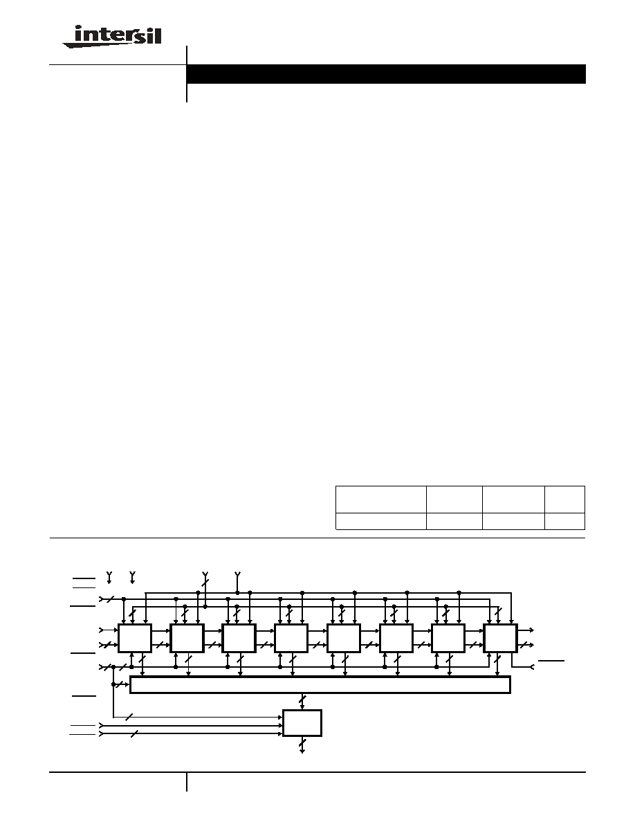
The HSP43881/883 is a video speed Digital Filter (DF)
designed to efficiently implement vector operations such as
FIR digital filters. It is comprised of eight filter cells cascaded
internally and a shift and add output stage, all in a single
integrated circuit. Each filter cell contains a 8 x 8-bit
multiplier, three decimation registers and a 26-bit
accumulator. The output stage contains an additional 26-bit
accumulator which can add the contents of any filter cell
accumulator to the output stage accumulator shifted right by
8-bits. The HSP43881/883 has a maximum sample rate of
25.6MHz. The effective multiply accumulate (mac) rate is
204MHz.
The HSP43881/883 DF can be configured to process
expanded coefficient and word sizes. Multiple DFs can be
cascaded for larger filter lengths without degrading the
sample rate or a single DF can process larger filter lengths
at less than 25.6MHz with multiple passes. The architecture
permits processing filter lengths of over 1000 taps with the
guarantee of no overflows. In practice, most filter coefficients
are less than 1.0, making even larger filter lengths possible.
The DF provides for 8-bit unsigned or two's complement
arithmetic, independently selectable for coefficients and
signal data.
Each DF filter cell contains three resampling or decimation
registers which permit output sample rate reduction at rates
of
1
/
2
,
1
/
3
or
1
/
4
the input sample rate. These registers also
provide the capability to perform 2-D operations such as
matrix multiplication and N x N spatial correlations/convolutions
for image processing applications.
Features
� This Circuit is Processed in Accordance to MIL-STD-883
and is Fully Conformant Under the Provisions of
Paragraph 1.2.1.
� 0MHz to 25.6MHz Sample Rate
� Eight Filter Cells
� 8-Bit Coefficients and Signal Data
� Low Power CMOS Operation
� I
CCSB
500
�
A Maximum
� I
CCOP
160mA Maximum at 20MHz
� 26-Bit Accumulator Per Stage
� Filter Lengths Up to 1032 Taps
� Expandable Coefficient Size, Data Size and Filter Length
� Decimation by 2, 3 or 4
Applications
� 1-D and 2-D FIR Filters
� Radar/Sonar
� Adaptive Filters
� Echo Cancellation
� Complex Multiply-Add
� Sample Rate Converters
Block Diagram
Ordering Information
PART NUMBER
TEMP.
RANGE (
o
C)
PACKAGE
PKG.
NO.
HSP43881GM-25/883
-55 to 125
85 Ld PGA
G85.A
TCCO
TCCI
CIN0 - 7
DF
FILTER
CELL 7
COUT0 - 7
ERASE
DCMO - 1
DIENB
CIENB
COENB
MUX
CLK
ADR0 - 2
RESET
26
ADR0, ADR1, ADR2
CLK
RESET
SHADD
SENBH
SENBL
OUTPUT
STAGE
8
V
CC
V
SS
DIN0 - DIN7 TCS
SUM0 - 25
3
8
DF
FILTER
CELL 6
26
8
8
DF
FILTER
CELL 5
26
8
8
DF
FILTER
CELL 4
26
8
8
DF
FILTER
CELL 3
26
8
8
DF
FILTER
CELL 2
26
8
8
DF
FILTER
CELL 1
26
8
8
DF
FILTER
CELL 0
26
8
8
8
5
5
2
26
26
2
8
5
Data Sheet
May 1999
CAUTION: These devices are sensitive to electrostatic discharge; follow proper IC Handling Procedures.
1-888-INTERSIL or 321-724-7143
|
Intersil (and design) is a trademark of Intersil Americas Inc.
Copyright � Intersil Americas Inc. 2002. All Rights Reserved
2
Pinouts
85 PIN PGA
TOP VIEW, PINS DOWN
A
B
C
D
E
F
G
H
J
K
L
2
1
7
3
4
5
6
8
9
10
11
COENB
RESET
DIN7
V
CC
DIN6
DIN3
DIN0
TCCI
V
CC
V
CC
COUT7
ERASE
DIN1
DIN2
CIENB
CIN7
CIN6
CIN4
COUT5
COUT6
ALIGN
PIN
DIENB
DIN5
DIN4
CIN5
CIN3
CIN2
V
CC
CIN1
CIN0
SENBL
COUT3
COUT4
COUT1
V
SS
COUT2
V
SS
COUT0
SHADD
ADR2
DCM0
CLK
SUM0
V
CC
V
SS
SUM1
SUM3
SUM2
SUM5
SUM4
ADR0
SUM25
V
CC
SUM7
V
SS
SUM16
SUM17
SUM20
SENBH
SUM24
V
SS
V
CC
SUM19
V
SS
SUM15
SUM12
SUM10
SUM8
SUM6
SUM9
SUM11
V
SS
SUM13
V
CC
SUM14
SUM18
SUM21
SUM22
SUM23
DCM1
V
SS
TCCO
TCS
ADR1
V
SS
HSP43881/883
3
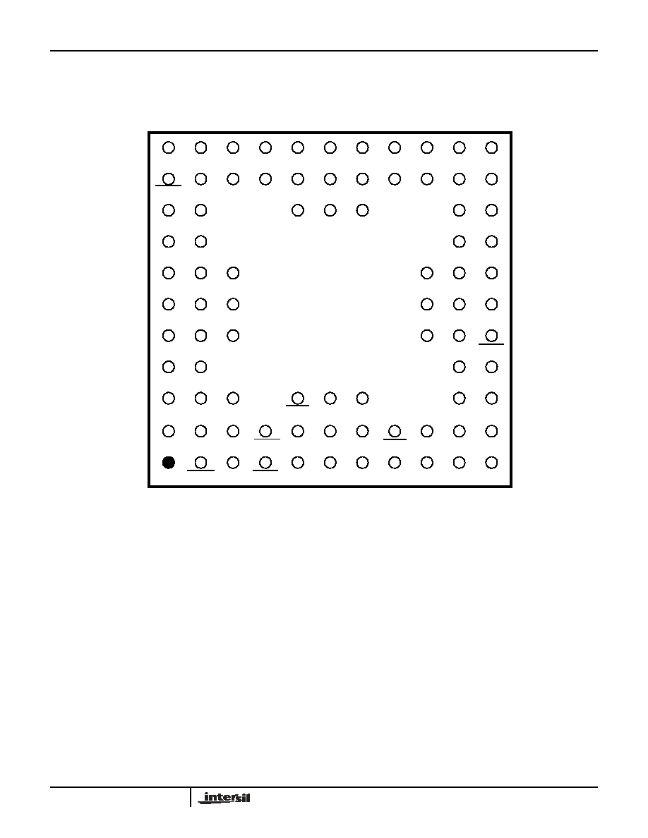
85 PIN PGA
BOTTOM VIEW, PINS UP
NOTE: An overbar on a signal name represents an active LOW signal.
Pinouts
(Continued)
DCM1
SUM23
SUM22
SUM21
SUM18
SUM14
SUM13
SUM11
SUM9
V
SS
V
CC
SUM20
SUM17
SUM16
SUM7
ADR0
SUM5
SUM4
ADR2
DCM0
CLK
V
SS
COUT0
SHADD
SUM1
SUM3
SUM2
SUM0
V
CC
V
SS
CIN2
V
CC
COUT3
COUT4
ALIGN
PIN
A
B
C
D
E
F
G
H
J
K
L
1
2
3
4
5
6
7
8
9
10
11
ADR1
SUM25
V
CC
V
SS
V
SS
V
CC
V
SS
SENBH
SUM24
SUM19
SUM15
SUM12
SUM10
SUM8
SUM6
CIN1
CIN0
SENBL
COUT1
V
SS
COUT2
COUT5
COUT6
DIENB
DIN5
DIN4
CIN5
CIN3
V
CC
V
SS
DIN0
DIN3
DIN6
DIN7
V
SS
COENB
V
CC
RESET
CIN8
V
CC
CIN4
CIN6
CIN7
CIENB
DIN2
DIN1
ERASE
COUT7
TCS
COUT8
HSP43881/883
4
Absolute Maximum Ratings
Thermal Information
Supply Voltage . . . . . . . . . . . . . . . . . . . . . . . . . . . . . . . . . . . . . 8.0V
Input, Output Voltage . . . . . . . . . . . . . . . . . . GND -0.5 to V
CC
+0.5V
ESD Rating . . . . . . . . . . . . . . . . . . . . . . . . . . . . . . . . . . . . . . Class 1
Operating Conditions
Voltage Range . . . . . . . . . . . . . . . . . . . . . . . . . . . . . . +4.5V to +5.5V
Temperature Range . . . . . . . . . . . . . . . . . . . . . . . . . -55
o
C to 125
o
C
Thermal Resistance (Typical, Note 1)
JA
(
o
C/W)
JC
(
o
C/W)
PGA Package. . . . . . . . . . . . . . . . . . . .
36.0
7.0
Maximum Package Power Dissipation at 125
o
C
PGA . . . . . . . . . . . . . . . . . . . . . . . . . . . . . . . . . . . . . . . . . . . 1.44W
Maximum Junction Temperature. . . . . . . . . . . . . . . . . . . . . . . . . . 175
o
C
Maximum Storage Temperate Range . . . . . . . . . . . -65
o
C to 150
o
C
Maximum Lead Temperature (Soldering 10s) . . . . . . . . . . . . .300
o
C
Die Characteristics
Gate Count . . . . . . . . . . . . . . . . . . . . . . . . . . . . . . . . . 17,762 Gates
CAUTION: Stresses above those listed in "Absolute Maximum Ratings" may cause permanent damage to the device. This is a stress only rating and operation of the
device at these or any other conditions above those indicated in the operational sections of this specification is not implied.
NOTE:
1.
JA
is measured with the component mounted on an evaluation PC board in free air.
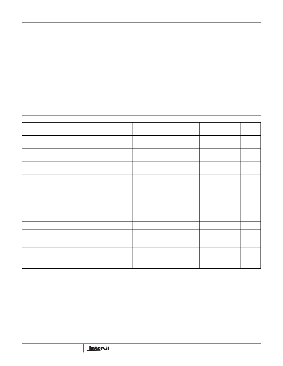
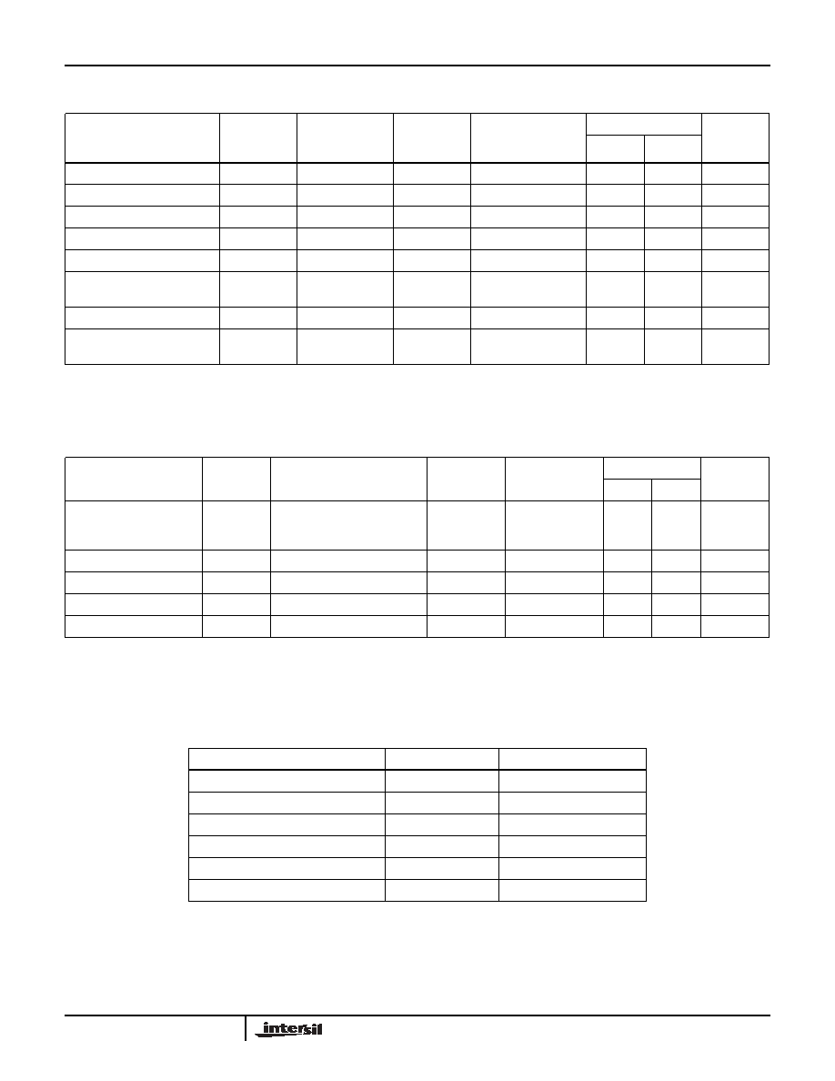
TABLE 1. DC ELECTRICAL PERFORMANCE SPECIFICATIONS
PARAMETER
SYMBOL
TEST
CONDITIONS
GROUP A
SUBGROUPS
TEMPERATURE
(
o
C)
MIN
MAX
UNITS
Logical One Input
Voltage
V
IH
V
CC
= 5.5V
1, 2, 3
-55
T
A
125
2.2
-
V
Logical Zero Input
Voltage
V
IL
V
CC
= 4.5V
1, 2, 3
-55
T
A
125
-
0.8
V
Output HIGH Voltage
V
OH
I
OH
= -400
�
A
V
CC
= 4.5V (Note 2)
1, 2, 3
-55
T
A
125
2.6
-
V
Output LOW Voltage
V
OL
I
OH
= -400mA
V
CC
= 4.5V (Note 2)
1, 2, 3
-55
T
A
125
-
0.4
V
Input Leakage Current
I
I
V
IN
= V
CC
or GND
V
CC
= 4.5V
1, 2, 3
-55
T
A
125
-10
+10
�
A
Output Leakage Current
I
O
V
IN
= V
CC
or GND
V
CC
= 5.5V
1, 2, 3
-55
T
A
125
-10
+10
�
A
Clock Input High
V
IHC
V
CC
= 5.5V
1, 2, 3
-55
T
A
125
3.0
-
V
Clock Input Low
V
ILC
V
CC
= 4.5V
1, 2, 3
-55
T
A
125
-
0.8
V
Standby Power Supply
Current
I
CCSB
V
IN
= V
CC
or GND
V
CC
= 5.5V,
Outputs Open
1, 2, 3
-55
T
A
125
-
500
�
A
Operating Power Supply
Supply Current
I
CCOP
f = 20.0MHz
V
CC
= 5.5V (Note 3)
1, 2, 3
-55
T
A
125
-
160.0
mA
Functional Test
FT
(Note 4)
7, 8
-55
T
A
125
-
-
NOTES:
2. Interchanging of force and sense conditions is permitted.
3. Operating supply current is proportional to frequency, typical rating is 8.0mA/MHz.
4. Tested as follows: f = 1MHz, V
IH
= 2.6, V
IL
= 0.4, V
OH
1.5V, V
OL
1.5V, V
IHC
= 3.4V and V
ILC
= 0.4V.
HSP43881/883
5
TABLE 2. AC ELECTRICAL PERFORMANCE SPECIFICATIONS
Device Guaranteed and 100% Tested
PARAMETER
SYMBOL
NOTES
GROUP A
SUBGROUP
S
TEMPERATURE
(
o
C)
-25 (25.6MHz)
UNITS
MIN
MAX
Clock Period
t
CP
Note 5
9, 10, 11
-55
T
A
125
39
-
ns
Clock Low
t
CL
Note 5
9, 10, 11
-55
T
A
125
16
-
ns
Clock High
t
CH
Note 5
9, 10, 11
-55
T
A
125
16
-
ns
Input Setup
t
IS
Note 5
9, 10, 11
-55
T
A
125
17
-
ns
Input Hold
t
IH
Note 5
9, 10, 11
-55
T
A
125
0
-
ns
CLK to Coefficient
Output Delay
t
ODC
Note 5
9, 10, 11
-55
T
A
125
-
20
ns
Output Enable Delay
t
OED
Note 5
9, 10, 11
-55
T
A
125
-
15
ns
CLK TO SUM
Output Delay
t
ODS
Note 5
9, 10, 11
-55
T
A
125
-
25
ns
NOTE:
5. AC Testing: V
CC
- 4.5V and 5.5V. Inputs are driven at 3.0V for a Logic "1" and 0.0V for a Logic "0". Input and output timing measurements are
made at 1.5V for both a Logic "1" an"). CLK is driven at 4.0V and 0V and measured at 2.0V.
TABLE 3. AC ELECTRICAL PERFORMANCE SPECIFICATIONS
PARAMETER
SYMBOL
TEST
CONDITIONS
NOTES
TEMP
(
o
C)
-25 (25.6MHz)
UNITS
MIN
MAX
Input Capacitance
C
IN
VCC = Open, f = 1MHz
All measurements are
referenced to device GND
6
T
A
= 25
-
15
pF
Output Capacitance
C
OUT
6
T
A
= 25
-
15
pF
Output Disable Delay
t
ODD
6, 7
-55
T
A
125
-
15
ns
Output Rise Time
t
OR
6, 7
-55
T
A
125
-
6
ns
Output Fall Time
t
OF
6, 7
-55
T
A
125
-
6
ns
NOTES:
6. The parameters listed in Table 3 are controlled via design or process parameters and are not directly tested. These parameters are characterized
upon initial design and after major process and/or design changes.
7. Loading is as specified in the test load circuit, C
L
= 40pF.
TABLE 4. APPLICABLE SUBGROUPS
CONFORMANCE GROUPS
METHOD
SUBGROUPS
Initial Test
100%/5004
-
Interim Test
100%/5004
-
PDA
100%
1
Final Test
100%
2, 3, 8A, 8B, 10, 11
Group A
-
1, 2, 3, 7, 8A, 8B, 9, 10, 11
Groups C and D
Samples/5005
1, 7, 9
HSP43881/883