 | –≠–ª–µ–∫—Ç—Ä–æ–Ω–Ω—ã–π –∫–æ–º–ø–æ–Ω–µ–Ω—Ç: HSP9501 | –°–∫–∞—á–∞—Ç—å:  PDF PDF  ZIP ZIP |
191
CAUTION: These devices are sensitive to electrostatic discharge; follow proper IC Handling Procedures.
http://www.intersil.com or 407-727-9207 | Copyright © Intersil Corporation 1999
HSP9501
Programmable Data Buffer
The HSP9501 is a 10-Bit wide programmable data buffer
designed for use in high speed digital systems. Two different
modes of operation can be selected through the use of the
MODSEL input. In the delay mode, a programmable data
pipeline is created which can provide 2 to 1281 clock cycles
of delay between the input and output data. In the data
recirculate mode, the output data path is internally routed
back to the input to provide a programmable circular buffer.
The length of the buffer or amount of delay is programmed
through the use of the 11-bit Length Control Input Port (LC0-
10) and the Length Control Enable (LCEN). An 11-bit value
is applied to the LC0-10 inputs, LCEN is asserted, and the
next selected clock edge loads the new count value into the
Length Control Register. The delay path of the HSP9501
consists of two registers with a programmable delay RAM
between them, therefore, the value programmed into the
Length Control Register is the desired length - 2. The range
of values which can be programmed into the Length Control
Register are from 0 to 1279, which in turn results in an
overall range of programmable delays from 2 to 1281.
Clock select logic is provided to allow the use of a positive or
negative edge system clock as the CLK input to the
HSP9501. The active edge of the CLK input is controlled
through the use of the CLKSEL input. All synchronous timing
(i.e., data setup, hold, and output delays) are relative to the
clock edge selected by CLKSEL. An additional clock enable
input (CLKEN) provides a means of disabling the internal
clock and holding the existing contents temporarily. All
outputs of the HSP9501 are three-state outputs to allow
direct interfacing to system or multi-use busses.
The HSP9501 is recommended for digital video processing
or any applications which require a programmable delay or
circular data buffer.
Features
∑ DC to 32MHz Operating Frequency
∑ Programmable Buffer Length from 2 to 1281 Words
∑ Supports Data Words to 10-Bits
∑ Clock Select Logic for Positive or Negative Edge
System Clocks
∑ Data Recirculate or Delay Modes of Operation
∑ Expandable Data Word Width or Buffer Length
∑ Three-State Outputs
∑ TTL Compatible Inputs/Outputs
∑ Low Power CMOS
Applications
∑ Sample Rate Conversion
∑ Data Time Compression/Expansion
∑ Software Controlled Data Alignment
∑ Programmable Serial Data Shifting
∑ Audio/Speech Data Processing Video/Image Processing
Video/Image Processing
∑ 1-H Delay Line of 910 NTSC, 1135 PAL or 1280 Samples:
- High Resolution Monitor Delay Line
- Comb Filter Designs
- Progressive Scanning Display
- TV Standards Conversion
- Image Processing
Ordering Information
PART NUMBER
TEMP.
RANGE (
o
C)
PACKAGE
PKG.
NO.
HSP9501JC-25
0 to 70
44 Ld PLCC
N44.65
HSP9501JC-32
0 to 70
44 Ld PLCC
N44.65
HSP9501JC-2596
0 to 70
44 Ld PLCC
Tape and Reel
N44.65
Data Sheet
January 1999
File Number
2786.4
192
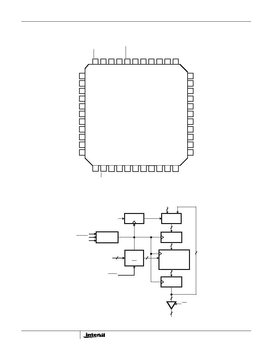
Pinout
44 LEAD PLCC
TOP VIEW
Block Diagram
CLKSEL
CLK
LC2
LC3
LC4
LC5
MODSEL
NC
NC
LCEN
CLK EN
DO9
OE
LC0
LC1
LC10
LC9
LC8
LC7
LC6
DI9
NC
40
6
5
3
2
1
44
43
42
41
4
18
19
20
21
22
23
24
25
26
27
28
7
17
16
15
12
13
14
9
10
11
8
38
37
39
35
34
33
36
31
30
29
32
DO0
DO1
DO2
DO3
DO4
GND
DO5
DO6
DO7
DO8
V
CC
DI0
DI1
DI2
DI3
DI4
GND
DI5
DI6
DI7
DI8
V
CC
MODSEL
MUX
CLOCK
GENERATOR
CLKSEL
CLK
CLKEN
11
REGISTER
REGISTER
EN
11
10
10
LC0 -10
OE
10
DO0-9
10
DI 0 -9
10
10
10
LCEN
REGISTER
PROGRAMMABLE
DELAY RAM
0-1279 DELAYS
REGISTER
HSP9501
193
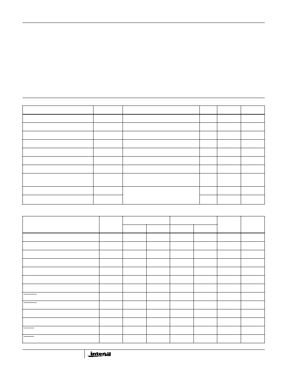
Pin Descriptions
NAME
PIN NUMBER
TYPE
DESCRIPTION
V
CC
12, 34
The +5V power supply pin. A 0.1
µ
F capacitor between the V
CC
and GND pin is
recommended.
GND
13, 33
The device ground.
CLK
1
I
Input Clock. This clock signal is used to control the data movement through the programmable buff-
er. It is also the signal which latches the input data, length control word and mode select. Input
setup and hold times with respect to the clock must be met for proper operation.
DIO-9
27, 29-32, 35-39
I
Data Inputs. This 10-bit input port is used to provide the input data. When MODSEL is low, data
on the DI0-9 inputs is latched on the clock edge selected by CLKSEL.
DO0-9
7-11, 14-18
O
Data Outputs. This 10-bit port provides the output data from the Internal Delay Registers. Data
latched into the DI0-9 inputs will appear at the DO0 9 outputs on the Nth clock cycle, where N is
the total delay programmed.
LC0-10
20-26, 41-44
I
Length Control Inputs. These inputs are used to specify the number of clock cycles of delay be-
tween the DI0-9 inputs and the DO0-9 outputs. An integer value between 0 and 1279 is placed on
the LC0-10 inputs, and the total delay length (N) programmed is the LC0-10 value plus 2. In order
to properly load an active length control word, the value must be presented to the LC0-10 inputs
and LCEN must be asserted during an active clock edge selected by CLKSEL.
LCEN
6
I
Length Control Enable. LCEN is used in conjunction with LC0-10 and CLK to load a new length
control word. An 11-bit value is loaded on the LC0-10 inputs, LCEN is asserted, and the next se-
lected clock edge will load the new count value. Since this operation is synchronous, LCEN must
meet the specified setup/hold times with respect to CLK for proper operation.
OE
19
I
Output Enable. This input controls the state of the DO0-9 output port. A low on this control line en-
ables the port for output. When OE is high, the output drivers are in the high impedance state. In-
ternal latching or transfer of data is not affected by this input.
MODSEL
40
I
Mode Select. This input is used to control the mode of operation of the HSP9501. A low on MOD-
SEL causes the device to latch new data at the DI0-9 inputs on every clock cycle, and operate as
a programmable pipeline register. When MODSEL is high, the HSP9501 is in the recirculate mode,
and will operate as a programmable length circular buffer. This control signal may be used in a syn-
chronous fashion during device operation, however, care must be taken to ensure the required set-
up/hold times with respect to CLK are met.
CLKSEL
5
I
Clock Select Control. This input is used to determine which edge of the CLK signal is used for con-
trolling all internal events. A low on CLKSEL selects the negative going edge, therefore, all setup,
hold, and output delay times are with respect to the negative edge of CLK. When CLKSEL is high,
the positive going edge is selected and all synchronous timing is with respect to the positive edge
of the CLK signal.
CLKEN
2
I
Clock Enable. This control signal can be used to enable or disable the CLK input. When low, the
CLK input is enabled and will operate in a normal fashion. A high on CLKEN will disable the CLK
input and will "hold'' all internal operations and data. This control signal may also be used in a syn-
chronous fashion, however, setup and hold requirements with respect to CLK must be met for prop-
er device operation. This signal takes effect on the clock following the one that latches it in.
HSP9501
194
Functional Description
The HSP9501 is a 10-bit wide programmable length data
buffer. The length of delay is programmable from 2 to 1281
delays in single delay increments.
Data into the delay line may be selected from the data input
bus (DI0-9) or as recirculated output, depending on the state
of the mode select (MODSEL) control input.
Mode Select
The MODSEL control pin selects the source of the data
moving into the delay line. When MODSEL is low, the data
input bus (DI0-9) is the source of the data. When MODSEL
is high, the output of the HSP9501 is routed back to the input
to form a circular buffer.
The MODSEL control line is latched at the input by the CLK
signal. The edge which latches this control signal is deter-
mined by the CLKSEL control line. In either case, the
MODSEL line is latched on one edge of the CLK signal with
the following edge moving data into and through the
HSP9501. Refer to the functional timing waveforms for
specific timing references.
Clock Select Logic
The clock select logic is provided to allow the use of positive
or negative edge system clocks. The active edge of the CLK
input to the HSP9501 is controlled through the use of the
CLKSEL input.
When CLKSEL is low, the negative going edge of CLK is
used to control all internal operations. A high on CLKSEL
selects the positive going edge of CLK.
All synchronous timing (i.e., setup, hold and output
propagation delay times are relative to the CLK edge
selected by CLKSEL. Functional timing waveforms for each
state of CLKSEL are provided (refer to Timing Waveforms for
details).
Delay Path Control
The HSP9501 buffer length is programmable from 2 to 1281
data words in one word increments. The minimum number of
delays which can be programmed is two, consisting of the
input and Output Buffer Registers only.
The length control inputs (LC0-10) are used to set the length
of the programmable delay ram which can vary in length
from 0 to 1279. The total length of the HSP9501 data buffer
will then be equal to the programmed value on LC0-10 plus
2. The programmed delay is established by the 11-bit integer
value of the LC0-10 inputs with LC-10 as the MSB and LC0
as the LSB.
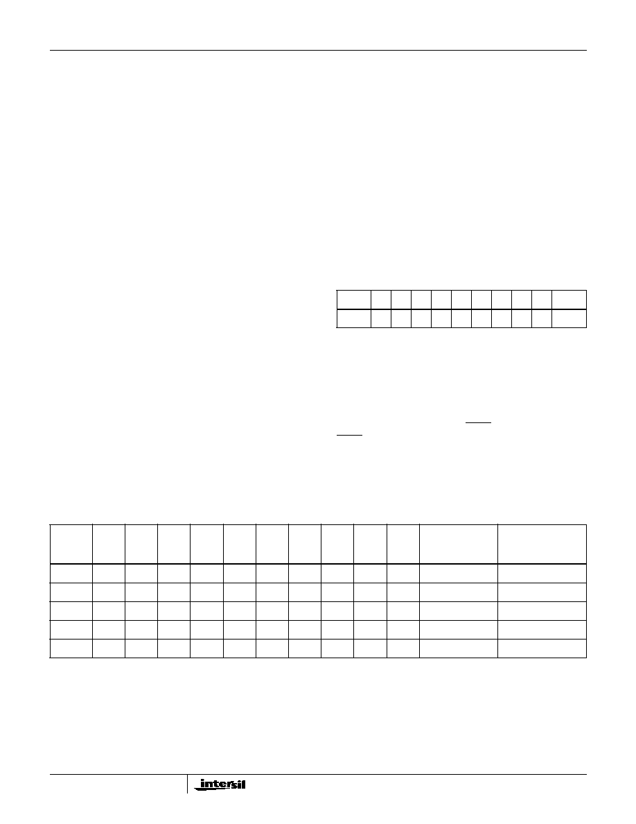
For example,
programs a length value of 2
6
+ 2
0
= 65. The total length of
the delay will be 65 + 2 or 67 delays.
Table 1 indicates several programming values. The decimal
value placed on LC0-10 must not exceed 1279. Controlled
operation with larger values is not guaranteed.
Values on LC0-10 are latched on the CLK edge selected by
the CLKSEL control line, when LCEN is active. LC0-10 and
LCEN must meet the specified setup and hold times relative
to the selected CLK edge for proper device operation.
LC10
9
8
7
6
5
4
3
2
1
LC0
0
0
0
0
1
0
0
0
0
0
1
TABLE 1. LENGTH CONTROL PROGRAMMING EXAMPLES
LC10 2
10
LC9
2
9
LS8
2
8
LC7
2
7
LC6
2
6
LC5
2
5
LC4
2
4
LC3
2
3
LC2
2
2
LC1
2
1
LC0
2
0
PROGRAMMED
LENGTH
TOTAL
LENGTH
N
0
0
0
0
0
0
0
0
0
0
0
0
2
0
0
0
0
1
1
1
0
1
1
0
118
120
0
1
1
0
0
1
0
1
0
0
0
808
810
1
0
0
0
0
0
1
1
0
0
1
1049
1051
1
0
0
1
1
1
1
1
1
1
1
1279
1281
HSP9501
195
Absolute Maximum Ratings
Thermal Information
Supply Voltage . . . . . . . . . . . . . . . . . . . . . . . . . . . . . . . . . . . . . +8.0V
Input, Output or Voltage Applied . . . . . . . . GND -0.5V to V
CC
+0.5V
Operating Conditions
Temperature Range . . . . . . . . . . . . . . . . . . . . . . . . . . . .0
o
C to 70
o
C
Voltage Range . . . . . . . . . . . . . . . . . . . . . . . . . . . . +4.75V to 5.25V
Thermal Resistance (Typical, Note 1)
JA
(
o
C/W)
PLCC Package . . . . . . . . . . . . . . . . . . . . . . . . . . . . .
45.2
Maximum Junction Temperature . . . . . . . . . . . . . . . . . . . . . . .150
o
C
Maximum Storage Temperature Range . . . . . . . . . . -65
o
C to 150
o
C
Maximum Lead Temperature (Soldering 10s) . . . . . . . . . . . . .300
o
C
(PLCC - Lead Tips Only)
CAUTION: Stresses above those listed in "Absolute Maximum Ratings" may cause permanent damage to the device. This is a stress only rating and operation of the
device at these or any other conditions above those indicated in the operational sections of this specification is not implied.
NOTE:
1.
JA
is measured with the component mounted on an evaluation PC board in free air.
DC Electrical Specifications
V
CC
= 5.0V +5%, T
A
= 0
o
C to 70
o
C, Commercial
PARAMETER
SYMBOL
TEST CONDITIONS
MIN
MAX
UNITS
Logical One Input Voltage
V
IH
V
CC
= 5.25V
2.0
-
V
Logical Zero Input Voltage
V
IL
V
CC
= 4.75V
-
0.8
V
Output HIGH Voltage
V
OH
I
OH
= -4mA V
CC
= 4.75V
2.4
-
V
Output LOW Voltage
V
OL
I
OL
= +4.0mA V
CC
= 4.75V
-
0.4
V
Input Leakage Current
I
I
V
IN
= GND or V
CC
V
CC
= 5.25V
-10
10
µ
A
Output Leakage Current
I
O
V
OUT
= GND or V
CC
= 5.25V
-10
10
µ
A
Standby Current
I
CCSB
V
IN
= V
CC
or GND, V
CC
= 5.25V, Note 3
-
500
µ
A
Operating Power Supply Current
I
CCOP
f = 25MHz, V
IN
= V
CC
or GND
V
CC
= 5.25V, Notes 2, 3
-
125
mA
Input Capacitance
C
IN
FREQ = 1MHz, V
CC
= Open, All
measurements are referenced to device
GND
-
10
pF
Output Capacitance
C
O
-
10
pF
AC Electrical Specifications
V
CC
= 5.0V
±
5%, T
A
= 0
o
C to +70
o
C, Commercial, (Note 5)
PARAMETER
SYMBOL
-32
-25
UNITS
NOTES
MIN
MAX
MIN
MAX
Clock Period
t
CP
31
-
40
-
ns
-
Clock Pulse Width High
t
PWH
12
-
15
-
ns
-
Clock Pulse Width Low
t
PWL
12
-
-
15
ns
-
Data Input Setup Time
t
DS
10
-
12
-
ns
-
Data Input Hold Time
t
DH
2
-
2
-
ns
-
Output Enable Time
t
ENA
-
20
-
25
ns
-
Output Disable Time
t
DIS
-
24
-
25
ns
Note 4
CLKEN to Clock Setup
t
ES
10
-
12
-
ns
-
CLKEN to Clock Hold
t
EH
2
-
2
-
ns
-
LC0-10 Setup Time
t
LS
10
-
13
-
ns
-
LC0-10 Hold Time
t
LH
2
-
2
-
ns
-
LCEN to Clock Setup
t
LES
10
-
13
-
ns
-
LCEN to Clock Hold
t
LEH
2
-
2
-
ns
-
HSP9501