ChipFind - документация

Электронный компонент: TB429

Скачать:  PDF   ZIP
1
TB429
CAUTION: These devices are sensitive to electrostatic discharge; follow proper IC Handling Procedures.
1-888-INTERSIL or 321-724-7143
|
Intersil (and design) is a registered trademark of Intersil Americas Inc.
Copyright Intersil Americas Inc. 2004. All Rights Reserved. Elantec is a registered trademark of Elantec Semiconductor, Inc.
All other trademarks mentioned are the property of their respective owners.
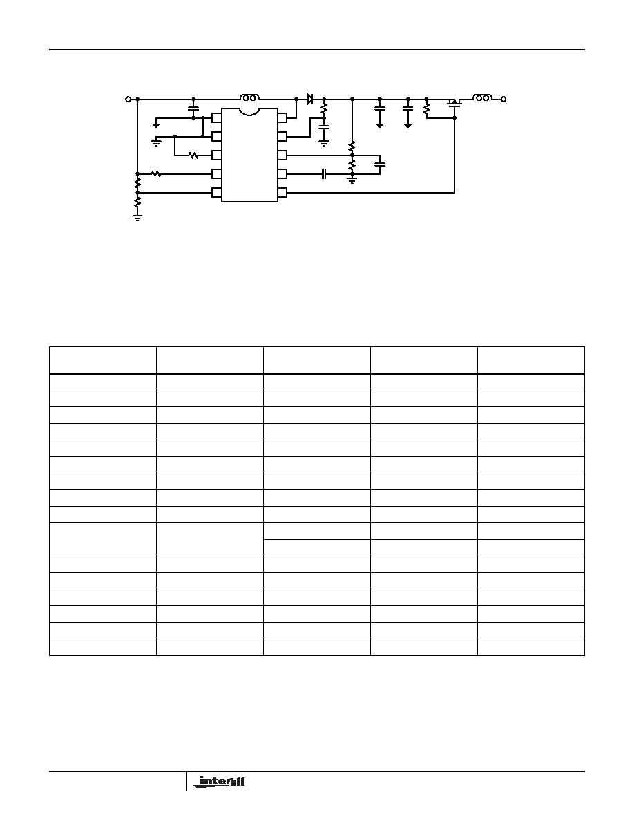
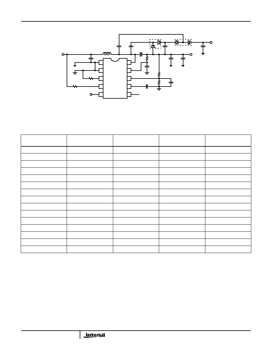
Using the EL7515 Demo Board
The complete schematic of EL7515
demo board is shown in Figure 1. With
different components stuffed, this
demo board can easily be configured into the applications
shown in this technical brief. The standard demo board
being sent out is the complete 5V to 12V converter shown in
Figure 2, which occupies less than 0.4 in
2
area with
components on top side only. Layout diagrams are given at
the end of this document.
1. V
IN
= 2V-5.5V. Can be higher with higher voltage rated
C
1
2. V
O
= 12V. Can be set according to the following formula:
where V
FB
is shown in the V
FB
vs V
DD
curve.
3. I
O
- up to 600mA depending on input voltage, provided
that diode and inductor can handle the corresponding
currents (refer to data sheet for the chart)
4. Switching frequency - can be set by R
3
5. R
4
can be 10
- 51 if V
O
is less than 10V. If V
O
is larger
than 12V, it can be calculated by:
where I
DD
is a function of switching frequency, as shown
in the I
DD
vs F
S
curve.
V
O
V
FB
1
R
2
R
1
-------
+
=
R
4
V
O
10
I
DD
---------------------
=
1
2
3
4
10
9
8
7
5
6
PGND
SGND
RT
EN
LBI
LX
VDD
FB
SS
LBO
C
3
R
1
R
2
C
5
C
6
C
4
R
4
D
1
L
1
C
1
R
3
V
IN
V
O11
C
7
R
7
R
8
R
6
EN
C
8
LBO
V
O1
L
2
C
12
C
13
V
O2
C
15
V
O3
V
O4
C
22
C
21
C
14
C
11
D
11
D
12
D
21
Q
1
R
9
FIGURE 1. COMPLETE SCHEMATIC OF EL7515 DEMO BOARD
FIGURE 2. 5V TO 12V CONVERTER
1
2
3
4
10
9
8
7
5
6
PGND
SGND
RT
EN
LBI
LX
VDD
FB
SS
LBO
C
3
R
1
R
2
C
5
C
6
C
4
R
4
D
1
L
1
C
1
R
3
V
IN
V
O1
C
10
R
6
Technical Brief
June 7, 2004
2
EL7515 Bill of Materials for V
O
=12V (Figure 2)
F
S
= 670kHz
REFERENCE
DESIGNATOR
VALUE
MANUFACTURER
MANUFACTURER'S
PHONE NUMBER
MANUFACTURER'S
PART NUMBER
R1
10k
/1%, 0603
Any
R2
82.5k
/1%, 0603
Any
R3
100k
, 0603
Any
R4
1k
, 0603
Any
R6
0
Any
C1
10F,16V, 1206
Murata
1-770-436-1300
GRM31CR61106KC31B
C3
20nF, 0603
Any
C4
0.1F/16V, 0805
Any
C5
22F, 16V, 1812
TDK
C4532X5R1C226M
C6
0.1F/16V, 0805
Any
C10
10nF, 0603
Any
L1
10H
Coilcraft
847-639-6400
DO1608C-103
D1
MBR0520
On Semiconductor
800-282-9855
MBR0520
EL7515 Bill of Materials for V
O
=18V (Figure 2)
F
S
= 1.2MHz
REFERENCE
DESIGNATOR
VALUE
MANUFACTURER
MANUFACTURER'S
PHONE NUMBER
MANUFACTURER'S
PART NUMBER
R1
10k
/1%, 0603
Any
R2
124k
Any
R3
47.5k
Any
R4
2.26k
Any
R6
0
Any
C1
10F, 16V, 1206
Murata
1-770-436-1300
GRM31CR61106KC31B
C3
20nF, 0603
Any
C4
0.1F/16V, 0805
Any
C5
22F, 16V, 1812
TDK
C4532X5R1C226M
C6
0.1F/16V, 0805
Any
C10
10nF
Any
L1
6.8H
Coilcraft
847-639-6400
DO1608C-682
D1
MBR0520
On Semiconductor
800-282-9855
MBR0520
Technical Brief 429
3
Disconnect voltage at:
FIGURE 3. EL7515 WITH OUTPUT DISCONNECT
1
2
3
4
10
9
8
7
5
6
PGND
SGND
RT
EN
LBI
LX
VDD
FB
SS
LBO
C
3
R
1
R
2
C
5
C
6
C
4
R
4
D
1
L
1
C
1
R
3
V
IN
(2.3V-3.7V)
V
O11
(4V,
400mA)
C
10
R
7
R
8
R
6
L
2
R
5
Q
1
V
IN
0.22
1
R
7
R
8
-------
+
=
EL7515 Bill of Materials for V
O
=4V (Figure 3)
F
S
= 670kHz
REFERENCE
DESIGNATOR
VALUE
MANUFACTURER
MANUFACTURER'S
PHONE NUMBER
MANUFACTURER'S
PART NUMBER
R1, R5, R8
10k
/1%, 0603
Any
R2
20k
/1%, 0603
Any
R3
100k
, 0603
Any
R4
51
, 0603
Any
R6
0
Any
R7
56.2k
Any
C1
10F, 16V, 1206
Murata
1-770-436-1300
GRM31CR61106KC31B
C3
20nF, 0603
Any
C4
0.1F/16V, 0805
Any
C5
330F
100F
Vishay/Sprague
207-324-4140
293D476X-020D20
Murata
1-770-436-1300
GRM43SR60J107M***B
C6
0.1F/16V, 0805
Any
C10
10nF, 0603
Any
L1
10H
Coilcraft
847-639-6400
DO1608C-103
L2
0
Any
D1
MBR0520
On Semiconductor
800-282-9855
MBR0520
Q1
IRLML6402
IR
IRLML6402
Technical Brief 429
4
1
2
3
4
10
9
8
7
5
6
PGND
SGND
RT
EN
LBI
LX
VDD
FB
SS
LBO
C
3
R
1
R
2
C
5
C
6
C
4
R
4
D
1
L
1
C
1
R
3
V
IN
(2.7V-
4.2V)
V
O1
(5.1V)
C
10
R
6
C
15
C
13
V
O3
(14.5V)
C
11
D
11
D
12
C
14
FIGURE 4. EL7515 WITH DUAL OUTPUTS
EL7515 Bill of Materials (Figure 4)
V
O1
= 5.1V, V
O3
= 14.5V, F
S
= 670kHz
REFERENCE
DESIGNATOR
VALUE
MANUFACTURER
MANUFACTURER'S
PHONE NUMBER
MANUFACTURER'S
PART NUMBER
R1
133k
/1%
Any
R2
402k
/1%
Any
R3
100k
Any
R4
51
Any
R6
0
Any
C1
10F, 16V, 1206
Murata
1-770-436-1300
GRM31CR61106KC31B
C3
20nF
Any
C4, C6, C11, C14
0.1F/16V
Any
C5
22F, 10V, 1210
Murata
1-770-436-1300
GRM32ER61A226KA65B
C10
10nF, 0603
Any
C13
1F
Any
C15
4.7F
Panasonic
408-945-5660
ECJ-3YF1C4752
L1
10H
Coilcraft
847-639-6400
DO1608C-103
D1
MBR0520
On Semiconductor
800-282-9855
MBR0520
D2, D3
BAT54S
Vishay/Telefunken
402-563-6866
BAT54S
Technical Brief 429
5
FIGURE 5. EL7515 FOR TRIPLE OUTPUT
1
2
3
4
10
9
8
7
5
6
PGND
SGND
RT
EN
LBI
LX
VDD
FB
SS
LBO
C
3
R
1
R
2
C
5
C
6
C
4
R
4
D
1
L
1
C
1
R
3
V
IN
C
10
R
6
C
12
V
O2
(19.5V)
V
O4
(~9.5V)
C
22
C
21
C
11
D
11
D
21
V
O1
(10V)
EL7515 Triple Output Bill of Materials (Figure 5)
V
O1
= 10V, V
O2
= 19.5V, V
O4
= -9.5V
REFERENCE
DESIGNATOR
VALUE
MANUFACTURER
MANUFACTURER'S
PHONE NUMBER
MANUFACTURER'S
PART NUMBER
R1
10k
/1%, 0603
Any
R2
66.5k
/1%, 0603
Any
R3
100k
, 0603
Any
R4
51
, 0603
Any
R6
0
Any
C1
10F, 16V, 1206
Murata
1-770-436-1300
GRM31CR61106KC31B
C3
20nF, 0603
Any
C4, C6, C11, C21
0.1F/16V, 0805
Any
C5
22F, 16V, 1812
TDK
C4532X5R1C226M
C10
10nF, 0603
Any
C12, C22
4.7F, 25V
Panasonic
408-945-5660
ECJ-3YF1C4752
L1
10H
Coilcraft
847-639-6400
DO1608C-153
D1
MBR0520
On Semiconductor
800-282-9855
MBR0520
D11, D21
BAT54S
Vishay/Telefunken
402-563-6866
BAT54S
Technical Brief 429
6
Typical Performance Curves
FIGURE 6. V
FB
vs V
DD
FIGURE 7. I
DD
vs F
S
1.355
1.35
1.345
1.34
1.335
1.33
1.325
1.32
5
6
7
8
9
11
12
V
DD
V
FB
10
3.6
3.4
3.2
3
2.8
2.6
2.4
2.2
2
650
750
850
950
1050
1150
1250
F
S
(kHz)
I
DD
(mA)
V
DD
=10V
V
O
=12V-18V
Technical Brief 429
7
Intersil Corporation reserves the right to make changes in circuit design, software and/or specifications at any time without notice. Accordingly, the reader is cautioned to
verify that the Application Note or Technical Brief is current before proceeding.
For information regarding Intersil Corporation and its products, see www.intersil.com
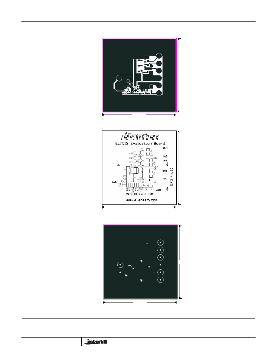
Demo Board Layout
FIGURE 8. TOP LAYER
2000 mil
2000 mil
FIGURE 9. TOP SILKSCREEN
2 in
2 in
FIGURE 10. BOTTOM LAYER
2000 mil
2000 mil
Technical Brief 429