50 A
90 A
100 A
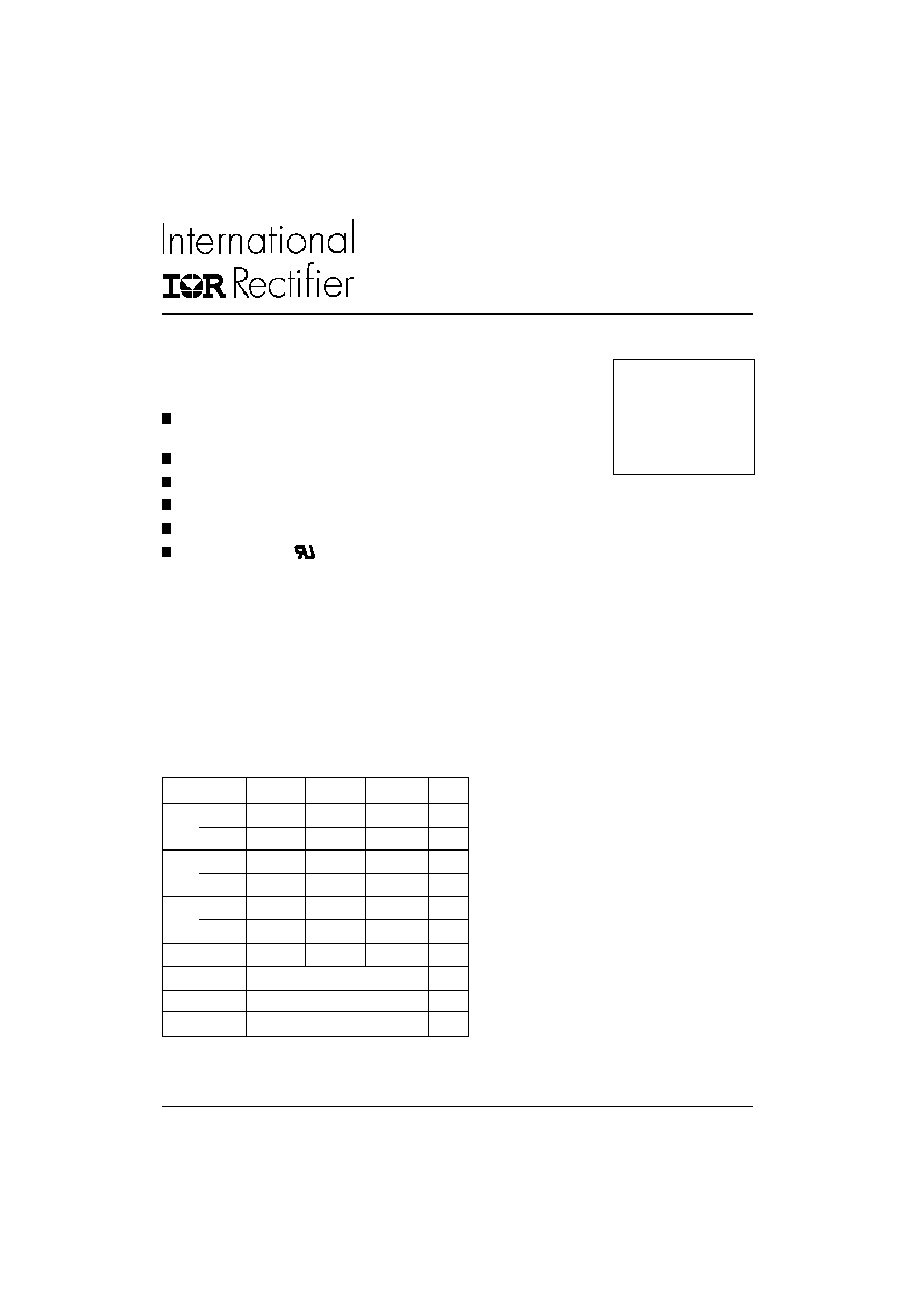
THREE PHASE AC SWITCH
Bulletin I27504 08/97
1
MT..KB SERIES
Power Modules
www.irf.com
Parameters
54MT.KB 94MT.KB 104MT.KB Units
I
O
50
90
100
A
@ T
C
80
80
80
∞C
I
FSM
@ 50Hz
390
950
1130
A
@ 60Hz
410
1000
1180
A
I
2
t
@ 50Hz
770
4525
6380
A
2
s
@ 60Hz
700
4130
5830
A
2
s
I
2
t
7700
45250
63800
A
2
s
V
RRM
range
800 to 1600
V
T
STG
range
- 40 to 125
∞C
T
J
range
- 40 to 125
∞C
Major Ratings and Characteristics
Features
Package fully compatible with the industry standard INT-A-pak
power modules series
High thermal conductivity package, electrically insulated case
Outstanding number of power encapsulated components
Excellent power volume ratio
4000 V
RMS
isolating voltage
UL E78996 approved
Description
A range of extremely compact, encapsulated three phase
AC-switches offering efficient and reliable operation. They
are intended for use in general purpose and heavy duty
applications as control motor starter.
54-94-104MT..KB Series
2
Bulletin I27504 08/97
www.irf.com
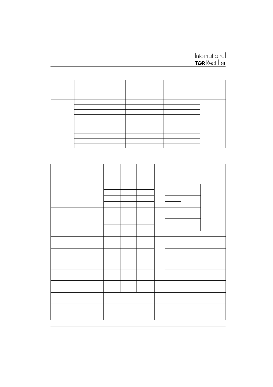
Voltage
V
RRM
, maximum
V
RSM
, maximum
V
DRM
, max. repetitive
I
RRM
/I
DRM
max.
Type number
Code
repetitive peak
non-repetitive peak
peak off-state voltage,
@ T
J
= 125∞C
reverse voltage
reverse voltage
gate open circuit
V
V
V
mA
80
800
900
800
100
1000
1100
1000
54MT..KB
120
1200
1300
1200
20 *
140
1400
1500
1400
160
1600
1700
1600
80
800
900
800
100
1000
1100
1000
94/104MT..KB
120
1200
1300
1200
40 *
140
1400
1500
1400
160
1600
1700
1600
Parameter
54MT.KB
94MT.KB 104MT.KB Units Conditions
I
O
Maximum I
RMS
output current
50
90
100
A
For all conduction angle
@ Case temperature
80
80
80
∞C
I
TSM
Maximum peak, one-cycle
390
950
1130
A
t = 10ms
No voltage
forward, non-repetitive
410
1000
1180
t = 8.3ms
reapplied
on state surge current
330
800
950
t = 10ms
100% V
RRM
345
840
1000
t = 8.3ms
reapplied
Initial
I
2
t
Maximum I
2
t for fusing
770
4525
6380
A
2
s
t = 10ms
No voltage
T
J
= T
J
max.
700
4130
5830
t = 8.3ms
reapplied
540
3200
4510
t = 10ms
100% V
RRM
500
2920
4120
t = 8.3ms
reapplied
I
2
t
Maximum I
2
t for fusing
7700
45250
63800
A
2
s
t = 0.1 to 10ms, no voltage reapplied
V
T(TO)1
Low level value of threshold
1.16
0.99
0.99
V
(16.7% x
x I
T(AV)
< I <
x I
T(AV)
), @ T
J
max.
voltage
V
T(TO)2
High level value of threshold
1.44
1.19
1.15
(I >
x I
T(AV)
), @ T
J
max.
voltage
r
t1
Low level value on-state
12.54
4.16
3.90
m
(16.7% x
x I
T(AV)
< I <
x I
T(AV)
), @ T
J
max.
slope resistance
r
t2
High level value on-state
11.00
3.56
3.48
(I >
x I
T(AV)
), @ T
J
max.
slope resistance
V
TM
Maximum on-state voltage drop
2.68
1.55
1.53
V
I
pk
= 150A, T
J
= 25∞C
t
p
= 400µs single junction
di/dt
Max. non-repetitive rate
150
A/µs
T
J
= 25
o
C, from 0.67 V
DRM
, I
TM
=
x I
T(AV)
,
of rise of turned on current
I
g
= 500mA,t
r
< 0.5 µs, t
p
> 6 µs
I
H
Max. holding current
200
T
J
= 25
o
C, anode supply = 6V,
mA
resistive load, gate open circuit
I
L
Max. latching current
400
T
J
= 25
o
C, anode supply = 6V, resistive load
Forward Conduction
ELECTRICAL SPECIFICATIONS
Voltage Ratings
* For single AC switch
54-94-104MT..KB Series
3
Bulletin I27504 08/97
www.irf.com
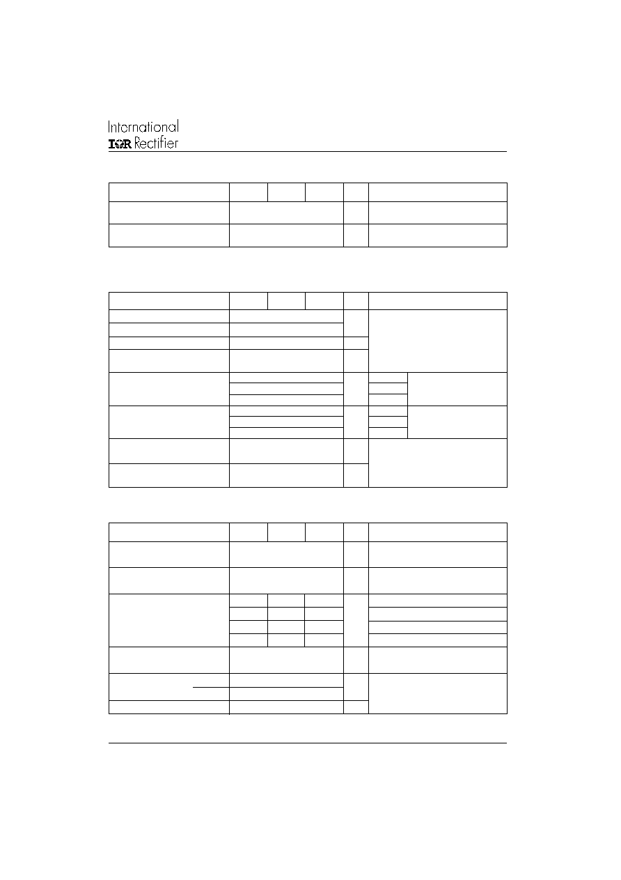
Parameter
54MT.KB 94MT.KB 104MT.KB Units Conditions
V
INS
RMS isolation voltage
4000
V
T
J
= 25
o
C all terminal shorted
f = 50Hz, t = 1s
dv/dt
Max. critical rate of rise
500
V/µs
T
J
= T
J
max., linear to 0.67 V
DRM
,
of off-state voltage (*)
gate open circuit
Blocking
(*) Available with dv/dt = 1000V/µs, to complete code add S90 i.e. 104MT160KBS90.
Triggering
Parameter
54MT.KB 94MT.KB 104MT.KB Units Conditions
P
GM
Max. peak gate power
10
W
T
J
= T
J
max.
P
G(AV)
Max. average gate power
2.5
I
GM
Max. peak gate current
2.5
A
-V
GT
Max. peak negative
10
V
gate voltage
V
GT
Max. required DC gate
4.0
V
T
J
= - 40∞C Anode supply = 6V, resistive load
voltage to trigger
2.5
T
J
= 25∞C
1.7
T
J
= 125∞C
I
GT
Max. required DC gate
270
T
J
= - 40∞C Anode supply = 6V, resistive load
current to trigger
150
mA
T
J
= 25∞C
80
T
J
= 125∞C
V
GD
Max. gate voltage
0.25
V
@ T
J
= T
J
max., rated V
DRM
applied
that will not trigger
I
GD
Max. gate current
6
mA
that will not trigger
Thermal and Mechanical Specifications
Parameter
54MT.KB 94MT.KB 104MT.KB Units Conditions
T
J
Max. junction operating
-40 to 125
∞C
temperature range
T
stg
Max. storage temperature
-40 to 125
∞C
range
R
thJC
Max. thermal resistance,
0.52
0.39
0.34
K/W
DC operation per single AC switch
junction to case
1.05
0.77
0.69
DC operation per junction
0.56
0.40
0.36
180∞ Sine cond. angle per single AC switch
1.12
0.80
0.72
180∞ Sine cond. angle per junction
R
thCS
Max. thermal resistance,
0.03
K/W
Per module
case to heatsink
Mounting surface smooth, flat and greased
T
Mounting
to heatsink
4 to 6
Nm
torque ± 10%
to terminal
3 to 4
wt
Approximate weight
225
g
A mounting compound is recommended and the
torque should be rechecked after a period of 3
hours to allow for the spread of the compound.
Lubricated threads.
54-94-104MT..KB Series
4
Bulletin I27504 08/97
www.irf.com
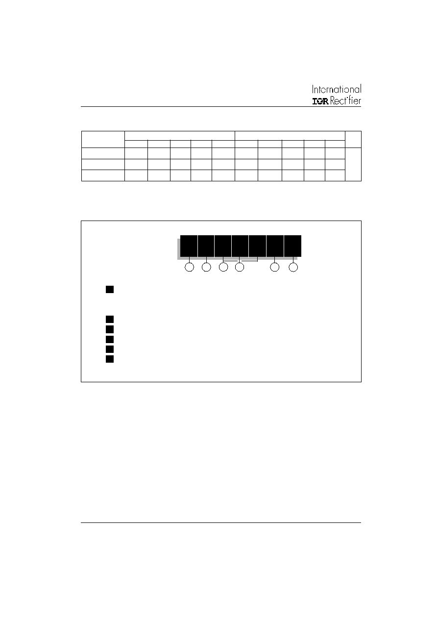
10
4
MT
160
K
B
S90
1
2
3
1
-
Current rating code: 5 = 50 A (Avg)
9 = 90 A (Avg)
10 = 100 A (Avg)
2
-
AC Switch
3
-
Essential part number
4
-
Voltage code: Code x 10 = V
RRM
(See Voltage Ratings Table)
5
-
Generation
II
6
-
Critical dv/dt: None = 500V/µs (Standard value)
S90
= 1000V/µs (Special selection)
4
Device Code
Ordering Information Table
5
6
Sinusoidal conduction @ T
J
max.
Rectangular conduction @ T
J
max.
Devices
Units
180
o
120
o
90
o
60
o
30
o
180
o
120
o
90
o
60
o
30
o
54MT.KB
0.072
0.085
0.108
0.152
0.233
0.055
0.091
0.117
0.157
0.236
K/W
94MT.KB
0.033
0.039
0.051
0.069
0.099
0.027
0.044
0.055
0.071
0.100
104MT.KB
0.027
0.033
0.042
0.057
0.081
0.023
0.037
0.046
0.059
0.082
R Conduction (per Junction)
(The following table shows the increment of thermal resistance R
thJC
when devices operate at different conduction angles than DC)
NOTE: To order the Optional Hardware see Bulletin I27900
54-94-104MT..KB Series
5
Bulletin I27504 08/97
www.irf.com
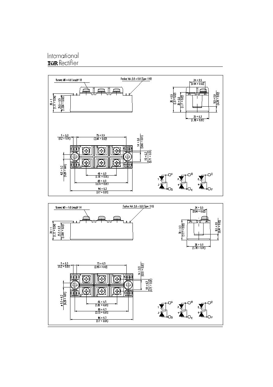
Outline Table (with optional barriers)
All dimensions in millimeters (inches)
Outline Table (without optional barriers)
All dimensions in millimeters (inches)