 | –≠–ª–µ–∫—Ç—Ä–æ–Ω–Ω—ã–π –∫–æ–º–ø–æ–Ω–µ–Ω—Ç: 10BF10 | –°–∫–∞—á–∞—Ç—å:  PDF PDF  ZIP ZIP |
SURFACE MOUNTABLE
ULTRAFAST RECOVERY DIODE
1
Preliminary Data Sheet PD-20482 rev. B 06/99
10BF.. Series
Major Ratings and Characteristics
Characteristics
10BF..
Units
10
20
40
60
80
I
F(AV)
1
A
V
RRM
100 to 800
V
I
FSM
30
A
V
F
@
1 A, T
J
= 25∞C
0.95
1.4
1.7
V
t
rr
@ T
J
= 25∞C
35
50
100
ns
T
J
range
- 50 to 150
∞C
Features
For surface mounted applications
Low profile package
Built-in stress relief
Compatible with all pick & place equipments
Ultrafast recovery times for high efficiency
Plastic package has Underwriters Laboratory
Flammability Classification 94V-O
Glass passivated junction
High temperature soldering:
260∞C\10 seconds at terminals
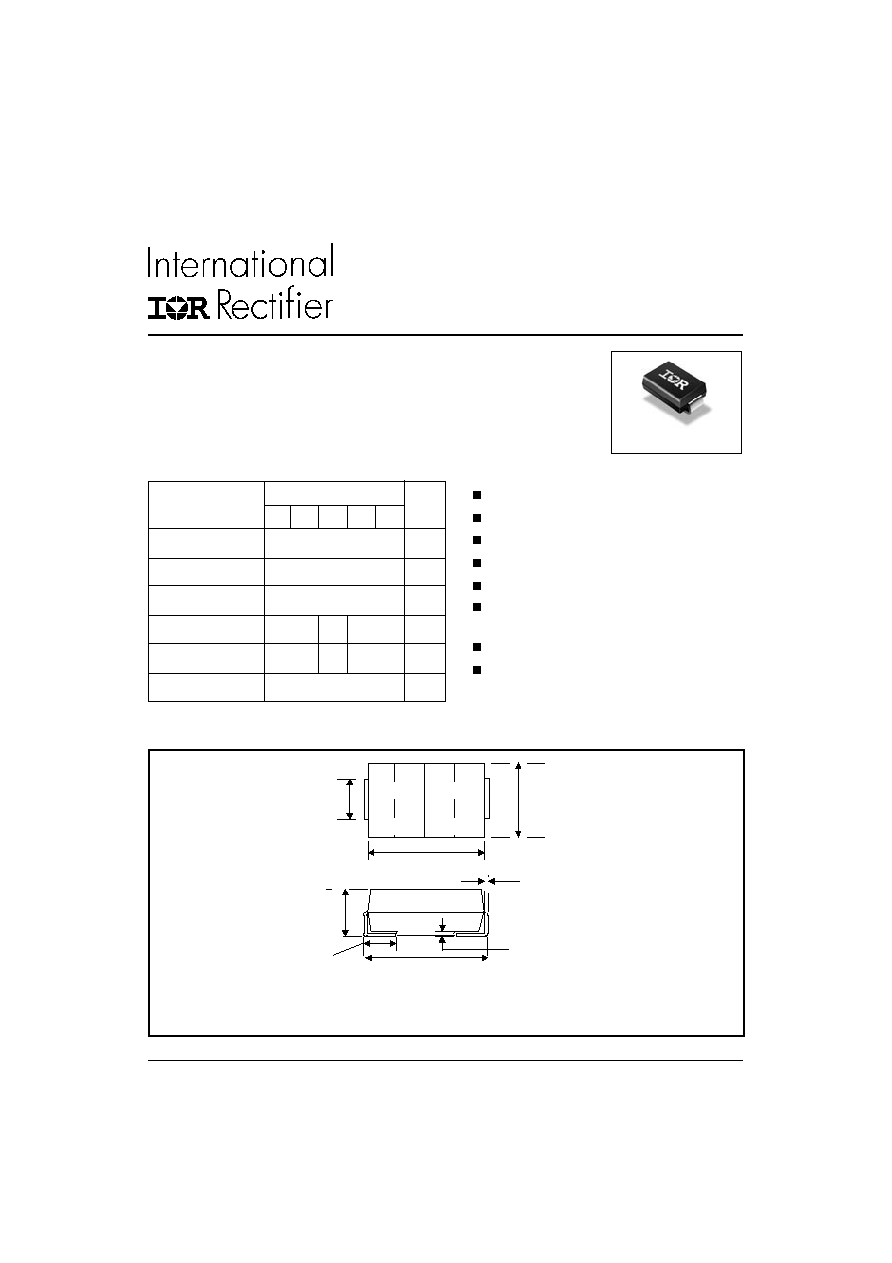
SMB (DO-214AA)
Dimensions in millimeters and (inches)
Outline SMB (DO-214AA)
3.30 (.130 )
3.94 (.155 )
4.06 (.160)
4.70 (.185)
1.91 (.075)
2.11 (.083)
.152 (.006)
.305 (.012)
2.13 (.083)
2.44 (.096)
0.76 (.030)
1.27 (.050)
.102 (.004)
.203 (.008)
5.08 (.200)
5.59 (.220)

2
10BF.. Series
Preliminary Data Sheet PD-20482 rev. B 06/99
V
RRM
, maximum
V
DC
, maximum
I
RRM
Part Number
peak reverse voltage
blocking voltage
100∞C
V
V
µA
10BF10
100
100
100
10BF20
200
200
10BF40
400
400
10BF60
600
600
10BF80
800
800
I
F(AV)
Maximum Average Forward Current
1
A
@ T
L
= 100∞ C
I
FSM
Peak Forward Surge Current
30
A
8.3ms single half sine wave superimposed
on rated load (JEDEC Method) T
A
= 55∞ C
V
FM
Max. Instantaneous Forward Voltage
0.95
1.4
1.7
V
@ 3A
I
RM
Maximum DC Reverse Current
10
µA
T
A
= 25∞ C
at Rated DC Blocking Voltage
100
T
A
= 100∞ C
t
rr
Reverse Recovery Time
35
50
100
ns
I
F
= 0.5A, I
R
= 1.0A, I
rr
= 0.25A
C
J
Typical Junction Capacitance
10
15
pf
@ 1.0MHz applied reverse voltage of 4.0 V
R
thJ
Maximum Thermal Resistance
35
30
∞C/W 8.0mm
2
(.013mm thick) land areas
T
J
Operating Temperature Range
- 50 to 150
∞C
T
stg
Storage Temperature Range
- 50 to 150
∞C
wt
Approximate Weight
0.21 (0.007)
g (oz)
Case Style
SMB/DO-214AA
JEDEC molded plastic
Voltage Ratings
Maximum Ratings and Electrical Characteristics
Parameters
10BF..
Units
Conditions
10
20
40
60
80
Ratings at 25∞C ambient temperature unless otherwise specified.
Resistive or inductive load.
For capacitive load, derate current by 20%.

3
10BF..
Series
Preliminary Data Sheet PD-20482 rev. B 06/99
Fig. 1 - Reverse Recovery Time Characteristic and Test Circuit Diagram
Fig. 2 - Typical Forward Characteristics
PULSE
GENERATOR
NOTE 2
OSCILLOSCOPE
NOTE 1
1
S
NON
INDUCTIVE
10
S
NON
INDUCTIVE
50
S
NON
INDUCTIVE
25 V dc
(a pprox)
(+)
(+)
(-)
(-)
D.U.T.
1c m
SET TIME
BASE FOR
10nsec/cm
+0.5A
0
-1 A
-0.25 A
trr
Fig. 4 - Forward Current Derating Curve
Fig. 5 - Peak Forward Surge Current
Fig. 3 - Typical Junction Capacitance
0.01
0.1
1
10
0
0.2
0.4
0. 6
0.8
1
1. 2
1.4
T = 25∞C
J
In
s
t
a
n
t
a
n
e
o
u
s
F
o
rw
a
r
d
C
u
rre
n
t
(
A
)
Instantaneous Forward Voltage (V)
Typical
10BF10/20
10BF40/60
10BF80
1
10
100
1000
0
20
40
60
80
100
R
T
J
u
n
c
t
i
o
n
Ca
p
a
c
i
t
a
n
c
e
-
C
(
p
F
)
10BF40/60/80
10BF10/20
Reverse Voltage - V (V)
1
10
100
1
10
100
FS
M
P
e
a
k
F
o
rw
a
r
d
S
u
rge
C
u
rre
n
t
-
I
(
A
)
Number of Cycles at 60HZ
8.3ms Single Half Sine Wave
JEDEC Method
50
60
70
80
90
100
110
120
130
140
150
0
0.2
0.4
0.6
0.8
1
1.2
F (AV)
Le
ad T
e
m
p
e
r
at
ur
e
-
(
∞C
)
Single phase half wave
60Hz resistive or inductive
load P.C.B. mounted
on 0.315x0.315" (8x8mm)
copper pad areas
Average Forward Current - I (A)

4
10BF.. Series
Preliminary Data Sheet PD-20482 rev. B 06/99
Ordering Information Table
10
B
F
80
Device Code
1
2
4
3
1
-
Current Rating x 10: 10 = 1A
2
-
B = DO-214AA (SMB) Surface Mount
3
-
F = Ultrafast Recovery
4
-
Voltage code: Code = V
RRM
/ 10
Tape & Reel Information
Dimensions in millimeters and (inches)