 | –≠–ª–µ–∫—Ç—Ä–æ–Ω–Ω—ã–π –∫–æ–º–ø–æ–Ω–µ–Ω—Ç: 121NQ | –°–∫–∞—á–∞—Ç—å:  PDF PDF  ZIP ZIP |
SCHOTTKY RECTIFIER
120 Amp
121NQ...(R) SERIES
Bulletin PD-2.249 rev. C 05/02
1
www.irf.com
Major Ratings and Characteristics
Description/Features
The 121NQ... (R) high current Schottky rectifier module
series has been optimized for low reverse leakage at high
temperature. The proprietary barrier technology allows for
reliable operation up to 175∞ C junction temperature. Typical
applications are in switching power supplies, converters,
free-wheeling diodes, and reverse battery protection.
175∞ C T
J
operation
Unique high power, Half-Pak module
Replaces two parallel DO-5's
Easier to mount and lower profile than DO-5's
High purity, high temperature epoxy encapsulation for
enhanced mechanical strength and moisture resistance
Low forward voltage drop
High frequency operation
Guard ring for enhanced ruggedness and long term
reliability
I
F(AV)
Rectangular
120
A
waveform
V
RRM
range
35 to 50
V
I
FSM
@ tp = 5 µs sine
19,800
A
V
F
@
120Apk, T
J
=125∞C
0.56
V
T
J
range
- 55 to 175
∞C
Characteristics
121NQ...(R) Units
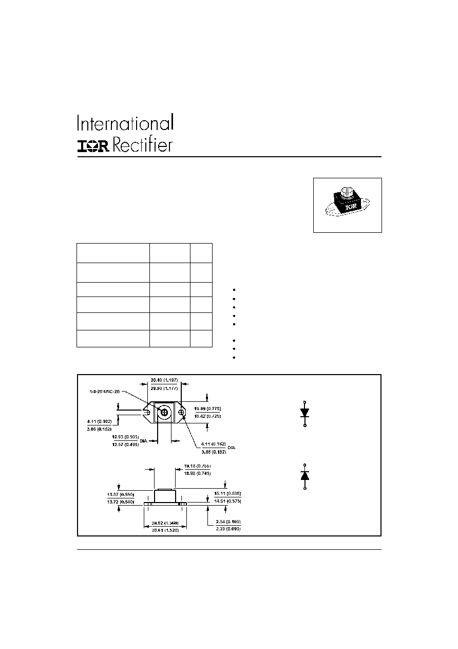
D-67
Outline D-67 HALF PAK Module
Dimensions in millimeters and (inches)
123NQ100
Lug Terminal Anode
Base Cathode
123NQ100R
Lug Terminal Cathode
Base Anode
121NQ...(R) Series
Bulletin PD-2.249 rev. C 05/02
2
www.irf.com
T
J
Max. Junction Temperature Range
-55 to 175
∞C
T
stg
Max. Storage Temperature Range
-55 to 175
∞C
R
thJC
Max. Thermal Resistance Junction
0.40
∞C/W DC operation * See Fig. 4
to Case
R
thCS
Typical Thermal Resistance, Case to
0.15
∞C/W Mounting surface , smooth and greased
Heatsink
wt
Approximate Weight
25.6 (0.9) g (oz.)
T
Mounting Torque
Min.
40 (35)
Non-lubricated threads
Max.
58 (50)
Terminal Torque
Min.
58 (50)
Max.
86 (75)
Case Style
HALF PAK Module
Thermal-Mechanical Specifications
Parameters
121NQ Units
Conditions
Kg-cm
(Ibf-in)
V
FM
Max. Forward Voltage Drop (1)
0.65
V
@ 120A
* See Fig. 1
0.83
V
@ 240A
0.56
V
@ 120A
0.70
V
@ 240A
I
RM
Max. Reverse Leakage Current (1)
10
mA
T
J
= 25 ∞C
* See Fig. 2
90
mA
T
J
= 125 ∞C
C
T
Max. Junction Capacitance
5200
pF
V
R
= 5V
DC
, (test signal range 100Khz to 1Mhz) 25 ∞C
L
S
Typical Series Inductance
7.0
nH
From top of terminal hole to mounting plane
dv/dt Max. Voltage Rate of Change
10000
V/ µs
(Rated V
R
)
T
J
= 25 ∞C
T
J
= 125 ∞C
V
R
= rated V
R
Parameters
121NQ Units
Conditions
(1) Pulse Width < 300µs, Duty Cycle < 2%
Electrical Specifications
I
F(AV)
Max. Average Forward Current
120
A
50% duty cycle @ T
C
= 133∞ C, rectangular wave form
* See Fig. 5
I
FSM
Max. Peak One Cycle Non-Repetitive
19,800
5µs Sine or 3µs Rect. pulse
Surge Current * See Fig. 7
2200
10ms Sine or 6ms Rect. pulse
E
AS
Non-Repetitive Avalanche Energy
81
mJ
T
J
= 25 ∞C, I
AS
= 12 Amps, L = 1.12 mH
I
AR
Repetitive Avalanche Current
12
A
Current decaying linearly to zero in 1 µsec
Frequency limited by T
J
max. V
A
= 1.5 x V
R
typical
Parameters
121NQ Units
Conditions
Absolute Maximum Ratings
A
Part number
121NQ035 121NQ040 121NQ045 121NQ050
V
R
Max. DC Reverse Voltage (V)
V
RWM
Max. Working Peak Reverse Voltage (V)
35
40
45
50
Voltage Ratings
Following any rated
load condition and
with rated V
RRM
applied
121NQ...(R) Series
Bulletin PD-2.249 rev. C 05/02
3
www.irf.com
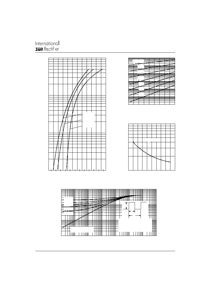
Fig. 2 - Typical Values of Reverse Current
Vs. Reverse Voltage
Fig. 3 - Typical Junction Capacitance
Vs. Reverse Voltage
Fig. 4 - Maximum Thermal Impedance Z
thJC
Characteristics
.001
.01
.1
1
10
100
1000
0
5 10 15 20 25 30 35 40 45
R
R
T = 175∞C
150∞C
125∞C
100∞C
75∞C
50∞C
25∞C
J
Reverse Voltage - V (V)
Re
v
e
r
s
e
C
u
rre
n
t
-
I
(m
A)
1000
10000
0
10
20
30
40
50
T = 25∞C
J
Reverse Voltage - V (V)
R
T
J
u
nc
t
i
on
C
ap
aci
t
an
ce
-
C
(p
F
)
.001
.01
.1
1
.00001
.0001
.001
.01
.1
1
10
100
D = 0.33
D = 0.50
D = 0.25
D = 0.17
D = 0.08
1
th
J
C
t , Rectangular Pulse Duration (Seconds)
Th
e
r
m
a
l
Im
p
e
d
a
n
c
e
-
Z
(
∞
C
/W
)
Single Pulse
(Thermal Resistance)
2
t
1
t
P
DM
Notes:
1. Duty factor D = t / t
2. Peak T = P x Z + T
1
J
DM thJC C
2
Fig. 1 - Maximum Forward Voltage Drop Characteristics
1
10
100
1000
0 .1 .2 .3 .4 .5 .6 .7 .8 .9 1 1.1 1.2
FM
F
In
s
t
a
n
ta
n
e
o
u
s
F
o
r
w
a
r
d
C
u
rre
n
t
- I
(A
)
T = 175∞C
T = 125∞C
T = 25∞C
J
J
J
Forward Voltage Drop - V (V)
121NQ...(R) Series
Bulletin PD-2.249 rev. C 05/02
4
www.irf.com
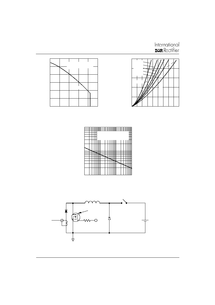
Fig. 8 - Unclamped Inductive Test Circuit
Fig. 5 - Maximum Allowable Case Temperature
Vs. Average Forward Current
Fig. 6 - Forward Power Loss Characteristics
Fig. 7 - Maximum Non-Repetitive Surge Current
0
20
40
60
80
100
0 20 40 60 80 100 120 140 160 180
DC
A
v
er
ag
e P
o
w
er
Lo
s
s
-
(
W
at
t
s
)
F(AV)
D = 0.08
D = 0.17
D = 0.25
D = 0.33
D = 0.50
RMS Limit
Average Forward Current - I (A)
120
130
140
150
160
170
180
0
40
80
120
160
200
DC
A
llo
w
a
b
l
e
C
a
s
e
T
e
m
p
e
r
a
t
u
re
-
(
∞
C
)
Average Forward Current - I (A)
F(AV)
121NQ
R (DC) = 0.40∞C/W
thJC
FRE E-W H EEL
D IO D E
40H FL40S02
C UR RE N T
M O N ITO R
H IG H -SPE ED
SW IT C H
IRFP460
L
D UT
R g = 2 5 oh m
V d = 25 V olt
+
1000
10000
100000
10
100
1000
10000
FS
M
p
Non-Repetitive Surge Current -
I (A)
At Any Rated Load Condition
And With Rated V Applied
Following Surge
RRM
Square Wave Pulse Duration - t (microsec)
121NQ...(R) Series
Bulletin PD-2.249 rev. C 05/02
5
www.irf.com
IR WORLD HEADQUARTERS: 233 Kansas St., El Segundo, California 90245, USA Tel: (310) 252-7105
TAC Fax: (310) 252-7309
Visit us at www.irf.com for sales contact information. 05/02
Data and specifications subject to change without notice.
This product has been designed and qualified for Industrial Level.
Qualification Standards can be found on IR's Web site.