Characteristics
12CWQ10FN Units
I
F(AV)
Rectangular
12
A
waveform
V
RRM
150
V
I
FSM
@ tp = 5µs sine
210
A
V
F
@6.0Apk, T
J
= 125∞C
0.75
V
(per leg)
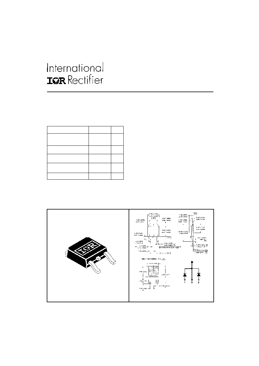
SCHOTTKY RECTIFIER
12 Amp
12CWQ150FN
The 12CWQ150FN surface mount, center tap, Schottky
rectifier has been designed for applications requiring low
forward drop and small foot prints on PC board. Typical
applications are in disk drives, switching power supplies,
converters, free-wheeling diodes, battery charging, and
reverse battery protection.
Popular D-PAK outline
Center tap configuration
Small foot print, surface mountable
Low forward voltage drop
High frequency operation
Guard ring for enhanced ruggedness and long term
reliability
Major Ratings and Characteristics
Desciption/Features
Preliminary Data Sheet PD-2.549 04/97
T
J
-55 to 175
∞C
CASE STYLE
D - PAK Outline (Similar to TO-252AA)
Dimensions in millimeters and inches
CATHODE
4
ANODE CATHODE ANODE
1
2
12CWQ150FN
Preliminary Data Sheet PD-2.549 04/97
Part number
12CWQ150FN
V
R
Max. DC Reverse Voltage (V)
V
RWM
Max. Working Peak Reverse Voltage (V)
Voltage Ratings
150
Parameters
12CWQ150FN
Units
Conditions
T
J
Max.Junction Temperature Range
-55 to 175
∞C
T
STG
Max. Storage Temperature Range
-55 to 175
∞C
R
thJC
Max. Thermal Resistance, Junction
3.0
∞C/W
DC operation
to case
R
thJA
Max. Thermal Resistance, Junction
110
DC operation
to Ambient
50
PC Board mounted print land = 20x20mm
wt
Approximate Weight
0.3(0.01) g (oz.)
Case Style
D-PAK
Similar to TO-252AA
Thermal-Mechanical Specifications
∞C/W
Parameters
12CWQ150FN
Units
Conditions
V
FM
Max. Forward Voltage Drop
0.75
V
@ 6.0A
(Per Leg)
(1)
I
RM
Max. Reverse Leakage Current
0.05
mA
T
J
= 25∞C
(Per Leg)
(1)
7.0
mA
T
J
= 125∞C
C
T
Max. Junction Capacitance (Per Leg)
100
pF
V
R
= 5V
DC
, ( test signal range 100Khz to 1Mhz),∞25 C
L
S
Typical Series Inductance (Per Leg)
5.0
nH
Measured lead to lead 5mm from package body
dv/dt
Max. Voltage Rate of Change
10,000
V
/ µs
(Rated V
R
)
T
J
= 125∞C
V
R
= rated V
R
Electrical Specifications
(1)
Pulse Width < 300µs, Duty Cycle < 2%
Parameters
12CWQ150FN
Units
Conditions
I
F(AV)
Max. Average Forward Current
50% duty cycle @ T
C
= 123∞C, rectangular waveform
I
FSM
Max. Peak One Cycle Non - Repetitive
210
5µs Sine or 3µs Rect. pulse
Surge Current (Per Leg)
42
10ms Sine 0r 6ms Rect. pulse
Absolute Maximum Ratings
Following any rated
load condition and with
rated V
RRM
applied
A
A
12
12CWQ150FN
Preliminary Data Sheet PD-2.549 04/97
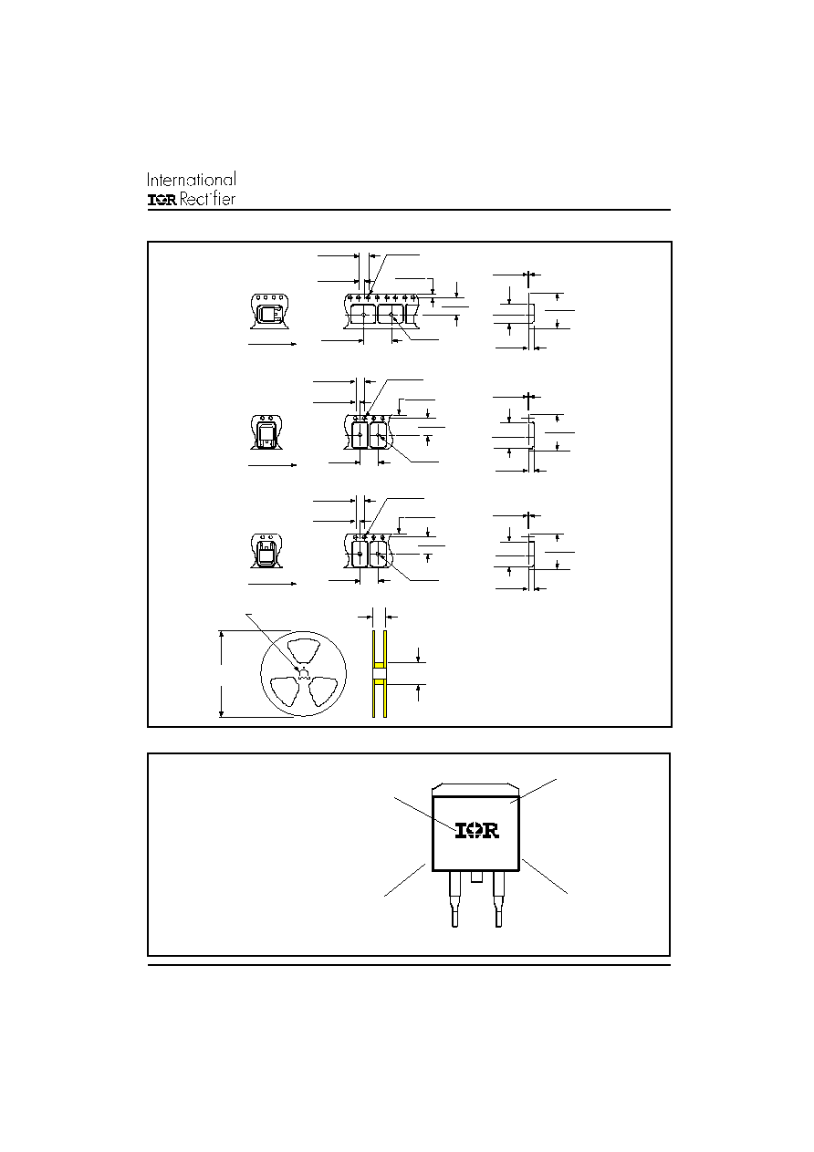
Tape & Reel Information
Part Marking Information
TR
FEED DIRECTION
4.1 (0.16)
3.9 (0.15)
2.1 (0.83)
1.9 (0.07)
12.1 (0.48)
1.65 (0.06)
1.85 (0.07)
1.65 (0.06)
7.4 (0.29)
2.6 (0.10)
1.5 (0.06)
7.6 (0.30)
11.9 (0.47)
1.85 (0.07)
TO-252AA Tape & Reel
When ordering, indicate the part
number, part orientation, and the
quantity. Quantities are in multiples
of 2,000 pieces per reel for TR and
multiples of 3,000 pieces per reel
for both TRL and TRR.
13 (0.52) DIA.
DIA. MAX.
375 (14.17)
50 (1.97) DIA.
22.4 (0.88)
0.35 (0.01)
16.3 (0.64)
15.7 (0.62)
2.75 (0.11)
2.55 (0.10)
0.25 (0.01)
6.8 (0.26)
7.0 (0.28)
TRR
FEED DIRECTION
4.1 (0.16)
3.9 (0.15)
2.1 (0.83)
1.9 (0.07)
8.1 (0.32)
1.85 (0.07)
1.65 (0.06)
1.85 (0.07)
1.65 (0.06)
7.4 (0.29)
2.6 (0.10)
1.5 (0.06)
7.6 (0.30)
7.9 (0.31)
0.35 (0.01)
16.3 (0.64)
15.7 (0.62)
2.75 (0.11)
2.55 (0.10)
0.25 (0.01)
10.4 (0.41)
10.6 (0.42)
DIA.
TRL
FEED DIRECTION
4.1 (0.16)
3.9 (0.15)
2.1 (0.83)
1.9 (0.07)
8.1 (0.32)
1.85 (0.07)
1.65 (0.06)
1.85 (0.07)
1.65 (0.06)
7.4 (0.29)
2.6 (0.10)
1.5 (0.06)
7.6 (0.30)
7.9 (0.31)
0.35 (0.01)
16.3 (0.64)
15.7 (0.62)
2.75 (0.11)
2.55 (0.10)
0.25 (0.01)
10.4 (0.41)
10.6 (0.42)
DIA.
DIA.
DIA.
DIA.
DIA.
EXAMPLE: THIS IS AN 12CWQ150FN
5K3A
12CWQ150FN
9712
INTERNATIONAL
RECTIFIER LOGO
PART NUMBER
DATE CODE (YYWW)
YY = YEAR
WW = WEEK
ASSEMBLY
LOT CODE
(K)
(A)
(A)