 | ÐлекÑÑоннÑй компоненÑ: 183NQ080 | СкаÑаÑÑ:  PDF PDF  ZIP ZIP |
Äîêóìåíòàöèÿ è îïèñàíèÿ www.docs.chipfind.ru
Major Ratings and Characteristics
Description/ Features
The 183NQ high current Schottky rectifier module series has
been optimized for low reverse leakage at high temperature.
The proprietary barrier technology allows for reliable opera-
tion up to 175° C junction temperature. Typical applications
are in switching power supplies, converters, free-wheeling
diodes, and reverse battery protection.
175° C T
J
operation
Unique high power, Half-Pak module
Replaces three parallel DO-5's
Easier to mount and lower profile than DO-5's
High purity, high temperature epoxy encapsulation for
enhanced mechanical strength and moisture resistance
Low forward voltage drop
High frequency operation
Guard ring for enhanced ruggedness and long term
reliability
I
F(AV)
Rectangular
180
A
waveform
V
RRM
range
80 to 100
V
I
FSM
@ tp = 5 µs sine
22,000
A
V
F
@
180Apk, T
J
=125°C
0.75
V
T
J
range
- 55 to 175
°C
Characteristics
183NQ...
Units
SCHOTTKY RECTIFIER
180 Amp
183NQ...(R) SERIES
Bulletin PD-2.256 rev. B 05/02
1
www.irf.com
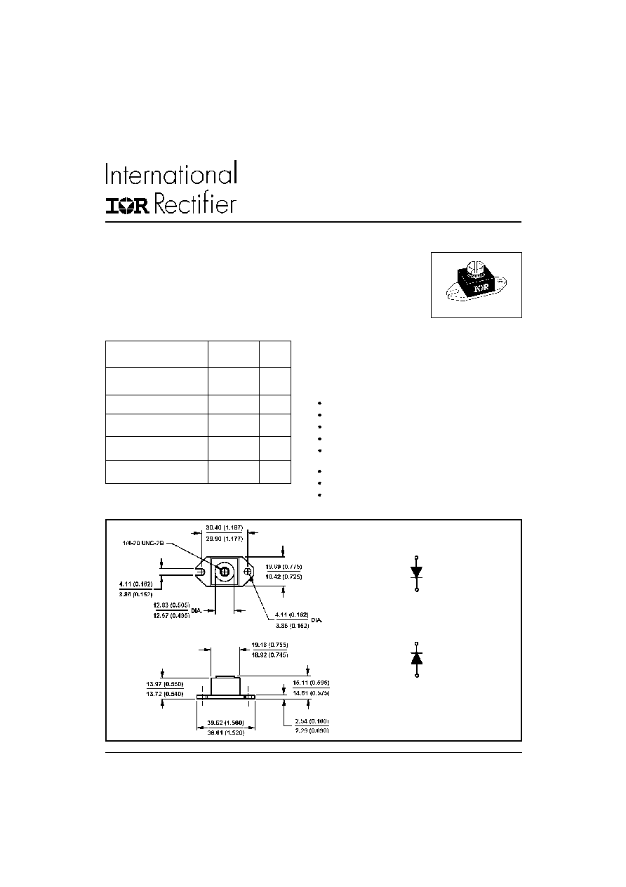
D-67
Outline D-67 HALF PAK Module
Dimensions in millimeters and (inches)
183NQ100
Lug Terminal Anode
Base Cathode
183NQ100R
Lug Terminal Cathode
Base Anode
183NQ...(R) Series
Bulletin PD-2.256 rev. B 05/02
2
www.irf.com
T
J
Max. Junction Temperature Range
-55 to 175
°C
T
stg
Max. Storage Temperature Range
-55 to 175
°C
R
thJC
Max. Thermal Resistance Junction
0.30
°C/W DC operation * See Fig. 4
to Case
R
thCS
Typical Thermal Resistance, Case to
0.15
°C/W Mounting surface , smooth and greased
Heatsink
wt
Approximate Weight
25.6 (0.9) g (oz.)
T
Mounting Torque
Min.
40 (35)
Non-lubricated threads
Max.
58 (50)
Terminal Torque
Min.
58 (50)
Max.
86 (75)
Case Style
HALF PAK Module
Thermal-Mechanical Specifications
Parameters
183NQ Units
Conditions
Kg-cm
(Ibf-in)
V
FM
Max. Forward Voltage Drop (1)
0.95
V
@ 180A
* See Fig. 1
1.14
V
@ 360A
0.75
V
@ 180A
0.89
V
@ 360A
I
RM
Max. Reverse Leakage Current (1)
4.5
mA
T
J
= 25 °C
* See Fig. 2
60
mA
T
J
= 125 °C
C
T
Max. Junction Capacitance
4150
pF
V
R
= 5V
DC
, (test signal range 100Khz to 1Mhz) 25 °C
L
S
Typical Series Inductance
6.0
nH
From top of terminal hole to mounting plane
dv/dt Max. Voltage Rate of Change
10000
V/ µs
(Rated V
R
)
T
J
= 25 °C
T
J
= 125 °C
V
R
= rated V
R
Parameters
183NQ Units
Conditions
(1) Pulse Width < 300µs, Duty Cycle < 2%
Electrical Specifications
I
F(AV)
Max. Average Forward Current
180
A
50% duty cycle @ T
C
= 116° C, rectangular wave form
* See Fig. 5
I
FSM
Max. Peak One Cycle Non-Repetitive
22,000
5µs Sine or 3µs Rect. pulse
Surge Current * See Fig. 7
1550
10ms Sine or 6ms Rect. pulse
E
AS
Non-Repetitive Avalanche Energy
15
mJ
T
J
= 25 °C, I
AS
= 1 Amps, L = 30 mH
I
AR
Repetitive Avalanche Current
1
A
Current decaying linearly to zero in 1 µsec
Frequency limited by T
J
max. V
A
= 1.5 x V
R
typical
Parameters
183NQ Units
Conditions
Absolute Maximum Ratings
A
Following any rated
load condition and
with rated V
RRM
applied
Part number
183NQ080
183NQ090
183NQ100
V
R
Max. DC Reverse Voltage (V)
V
RWM
Max. Working Peak Reverse Voltage (V)
Voltage Ratings
80
90
100
183NQ... Series
Bulletin PD-2.256 rev. B 05/02
3
www.irf.com
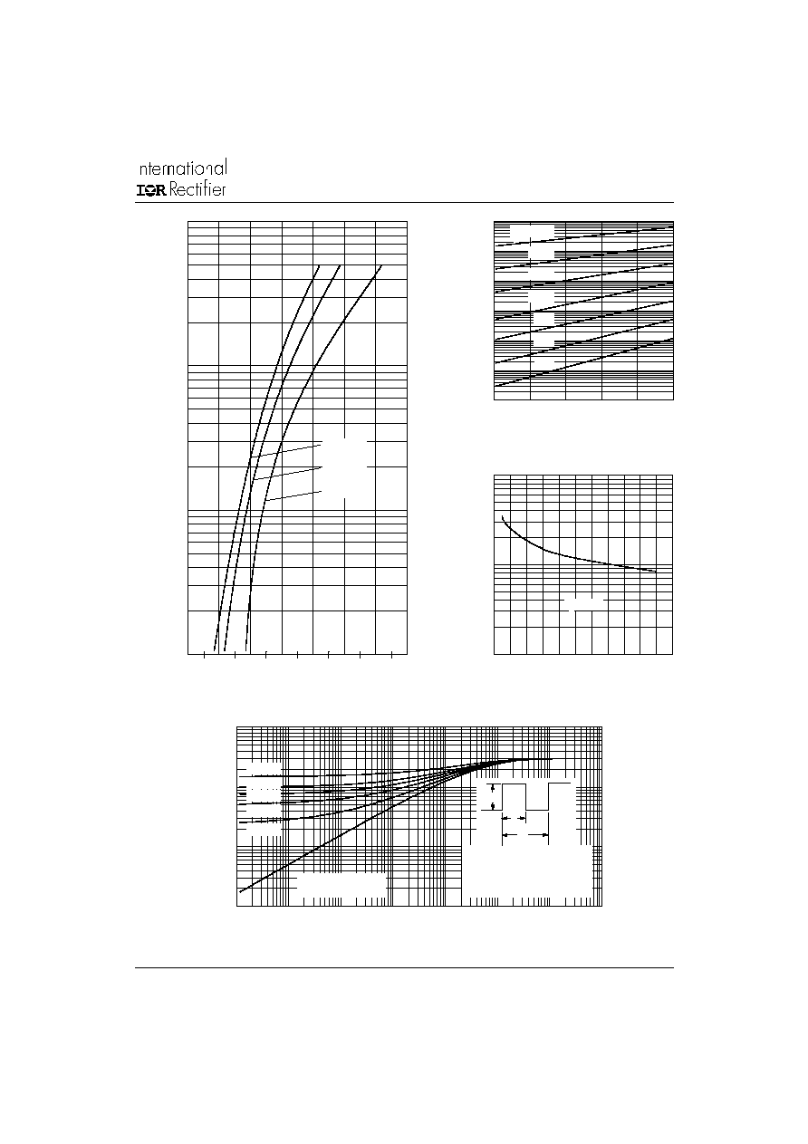
Fig. 2 - Typical Values of Reverse Current
Vs. Reverse Voltage
Fig. 3 - Typical Junction Capacitance
Vs. Reverse Voltage
Fig. 4 - Maximum Thermal Impedance Z
thJC
Characteristics
Fig. 1 - Maximum Forward Voltage Drop Characteristics
1
10
100
1000
0
.2
.4
.6
.8
1
1.2
1.4
FM
F
In
s
t
a
n
ta
n
e
o
u
s
F
o
r
w
a
r
d
C
u
r
r
e
n
t
-
I (
A
)
T = 175°C
T = 125°C
T = 25°C
J
J
J
Forward Voltage Drop - V (V)
.001
.01
.1
1
10
100
1000
0
20
40
60
80
100
R
R
T = 175°C
150°C
125°C
100°C
75°C
50°C
25°C
J
Reverse Voltage - V (V)
R
ev
e
r
s
e
C
u
r
r
e
n
t
-
I (
m
A)
100
1000
10000
0 10 20 30 40 50 60 70 80 90100110
T = 25°C
J
Reverse Voltage - V (V)
R
T
J
u
n
c
ti
o
n
C
a
p
a
c
i
ta
n
c
e
-
C
(
p
F
)
.001
.01
.1
1
.00001
.0001
.001
.01
.1
1
10
100
D = 0.33
D = 0.50
D = 0.25
D = 0.17
D = 0.08
1
th
J
C
t , Rectangular Pulse Duration (Seconds)
Th
e
r
m
a
l
Im
p
e
d
a
n
c
e
-
Z
(
°
C
/W
)
Single Pulse
(Thermal Resistance)
2
t
1
t
P
DM
Notes:
1. Duty factor D = t / t
2. Peak T = P x Z + T
1
J
DM thJC C
2
183NQ...(R) Series
Bulletin PD-2.256 rev. B 05/02
4
www.irf.com
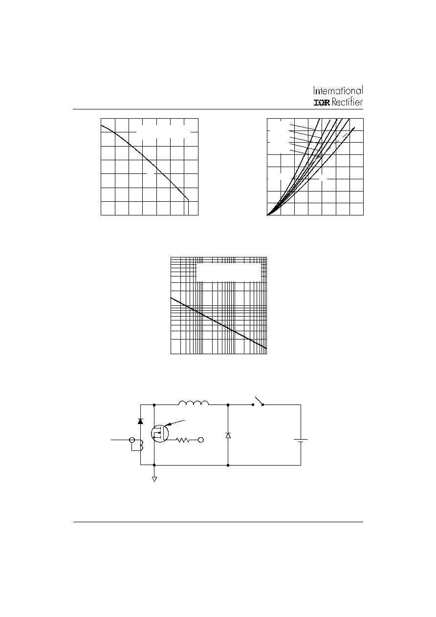
Fig. 8 - Unclamped Inductive Test Circuit
Fig. 5 - Maximum Allowable Case Temperature
Vs. Average Forward Current
Fig. 6 - Forward Power Loss Characteristics
Fig. 7 - Maximum Non-Repetitive Surge Current
110
120
130
140
150
160
170
180
0
40
80
120 160 200 240 280
DC
Al
l
o
w
ab
l
e
C
as
e
T
e
m
p
e
ra
tu
r
e
-
(
°
C
)
Average Forward Current - I (A)
F(AV)
183NQ
R (DC) = 0.30°C/W
thJC
0
25
50
75
100
125
150
175
200
0
40
80 120 160 200 240 280
DC
A
v
e
r
ag
e P
o
w
e
r
L
o
s
s
- (W
a
tts
)
F(AV)
D = 0.08
D = 0.17
D = 0.25
D = 0.33
D = 0.50
RMS Limit
Average Forward Current - I (A)
1000
10000
100000
10
100
1000
10000
FS
M
p
Non-Repetitive Surge Current -
I (A)
At Any Rated Load Condition
And With Rated V Applied
Following Surge
RRM
Square Wave Pulse Duration - t (microsec)
FRE E-W H EEL
D IO D E
40H FL40S02
C UR RE N T
M O N ITO R
H IG H -SPE ED
SW IT C H
IRFP460
L
D UT
R g = 2 5 oh m
V d = 25 V olt
+
183NQ... Series
Bulletin PD-2.256 rev. B 05/02
5
www.irf.com
IR WORLD HEADQUARTERS: 233 Kansas St., El Segundo, California 90245, USA Tel: (310) 252-7105
TAC Fax: (310) 252-7309
Visit us at www.irf.com for sales contact information. 05/02
Data and specifications subject to change without notice.
This product has been designed and qualified for Industrial Level.
Qualification Standards can be found on IR's Web site.